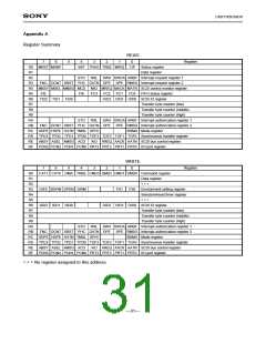
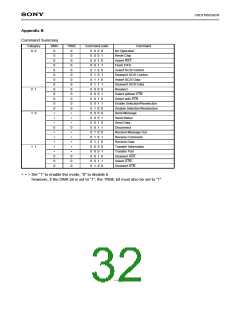
CXD1185CQ/CR
6-2. Target mode
<Initial setting>
Refer to the paragraph for initial settings in initiator mode.
<Switching to arbitration/selection>
4
5
SCSI ID setting
Write owner ID to the SCSI ID register.
Arbitration/selection
Write “1”s to at least SWA, SWOA and FNC bits etc. in the interrupt authorization registers 1 and 2. Wait
for the initiator to complete arbitration and to begin selection. If selected, either SWA or SWOA (but, not
both) is set in the interrupt request register. If ATN was active during selection, SWA is set.
Approximately 10 µs later, FNC is set in the interrupt request register 2 and only then D1185A enters
target mode.
<Message out phase execution>
6
Message out phase execution
Write “Receive Message Out” command into the command register (in order to read 1 byte of the
message DMA and TRBE bits should, both, be “0”). When bit 0 (CIP) of the status register becomes “0”,
read interrupt request registers 1 and 2.
7
Receiving message byte
At this point message is already in the data register. Read the data register and analyze it. If there is
more than 1 byte of message to be received, repeat 5 and 6.
<Command phase execution>
8
ACK signal confirmation
Before the initiator inactivate ACK signal on SCSI bus, message byte is already fed inside FIFO. Before
executing the next command, it is necessary to confirm that MACK bit in the SCSI control monitor register
is “0”.
9
Command phase execution
Write “6” to the transfer byte counter, and write “Receive Command” (DMA bit is at “0” and TRBE bit is at
“1”) command to the command register. Read interrupt request registers 1 and 2 when bit 0 (CIP) of the
status register becomes “0”.
10 Receive command byte
6 bytes of command data are stored in the data register. Read the data register and analyze them. If it is
necessary to receive a larger number of command data, repeat 8 and 9.
<Data in phase execution>
11 ACK signal confirmation
It is necessary to confirm that MACK bit in the SCSI control monitor register is “0”.
12 Data phase execution
Set the number of transfer data (in bytes) in the transfer byte counter. Write “Send Data” (both DMA and
TRBE bits are at “1”) command in the command register. When CIP bit is “0”, read interrupt request
registers 1 and 2.
—29—

 SONY [ SONY CORPORATION ]