Highly Integrated Full Featured Hi-Speed USB 2.0 ULPI Transceiver
Datasheet
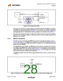
5.4.3
REFCLK Jitter
The USB3320 is tolerant to jitter on the reference clock. The REFCLK jitter should be limited to a peak
to peak jitter of less than 1nS over a 10uS time interval. If this level of jitter is exceeded when
configured for either ULPI Input Clock Mode or ULPI Output Clock Mode, the USB3320 Hi-Speed eye
diagram may be degraded.
The frequency accuracy of the REFCLK must meet the +/- 500ppm requirement as shown in Table 4.2.
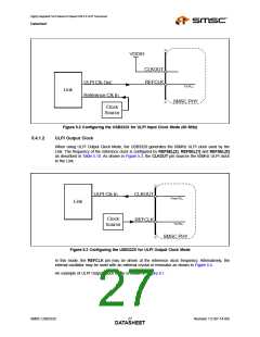
5.4.4
REFCLK Enable/Disable
The REFCLK should be enabled when the RESETB pin is brought high. The ULPI interface will start
running after the time specified in Table 4.2. If the REFCLK enable is delayed relative to the RESETB
pin, the ULPI interface will start operation delayed by the same amount. The REFCLK can be run at
anytime the RESETB pin is low without causing the USB3320 to start-up or draw current.
When the USB3320 is placed in Low Power Mode or Carkit Mode, the REFCLK can be stopped after
the final ULPI register write is complete. The STP pin is asserted to bring the USB3320 out of Low
Power Mode. The REFCLK should be started at the same time STP is asserted to minimize the
USB3320 start-up time.
If the REFCLK is stopped while CLKOUT is running, the PLL will come out of lock and the frequency
of the CLKOUT signal will decrease to the minimum allowed by the PLL design. If the REFCLK is
stopped during a USB session, the session may drop.
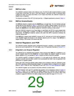
5.5
Internal Regulators and POR
The USB3320 includes integrated power management functions, including a Low-Dropout regulator
that can be used to generate the 3.3V USB supply, and a POR generator described in Section 5.5.2.
5.5.1
Integrated Low Dropout Regulator
The USB3320 has an integrated linear regulator. Power sourced at the VBAT pin is regulated to 3.3V
and the regulator output is on the VDD33 pin. To ensure stability, the regulator requires an external
bypass capacitor (COUT) as specified in Table 4.9 placed as close to the pin as possible.
The USB3320 regulator is designed to generate a 3.3 volt supply for the USB3320 only. Using the
regulator to provide current for other circuits is not recommended and SMSC does not guarantee USB
performance or regulator stability.
During USB UART mode the regulator output voltage can be changed to allow the USB3320 to work
with UARTs operating at different operating voltages. The regulator output is configured to the voltages
shown in Table 4.9 with the UART RegOutput[1:0] bits in the USB IO & Power Management register.
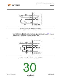
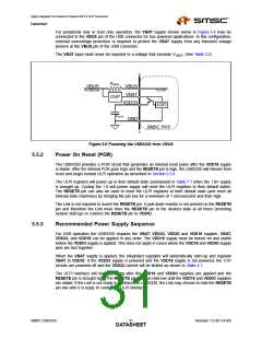
The USB3320 regulator can be powered in the three methods as shown below.
For USB Peripheral, Host, and OTG operations the regulator can be connected as shown in Figure 5.6
or Figure 5.7 below. For OTG operation, the VDD33 supply on the USB3320 must be powered to
detect devices attaching to the USB connector and detect a SRP during an OTG session. When using
a battery to supply the USB3320, the battery voltage must be within the range of 3.1V to 5.5V.
SMSC USB3320
Revision 1.0 (07-14-09)
DATA2S9HEET

 SMSC [ SMSC CORPORATION ]