Highly Integrated Full Featured Hi-Speed USB 2.0 ULPI Transceiver
Datasheet
~
~
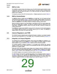
ULPI Clk In
CLKOUT
REFCLK
From PLL
Link
Internal
To PLL
Oscillator
Resonator
XO
- or -
~
~
Crystal
SMSC PHY
and Caps
CLOAD
Figure 5.4 ULPI Output Clock Mode
After the PLL has locked to the correct frequency, the USB3320 generates the 60MHz ULPI clock on
the CLKOUT pin, and de-asserts DIR to indicate that the PLL is locked. The USB3320 is guaranteed
to start the clock within the time specified in Table 4.2, and it will be accurate to within ±500ppm. For
Host applications the ULPI AutoResume bit should be enabled. This is described in Section 6.2.4.4.
When using ULPI Output Clock Mode, the edges of the reference clock do not need to be aligned in
any way to the ULPI interface signals; in other words, there is no need to align the phase of the
REFCLK and the CLKOUT.
5.4.2
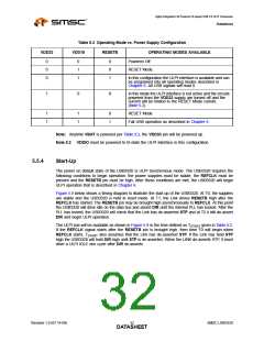
REFCLK Amplitude
The reference clock is connected to the REFCLK pin as shown in the application diagrams, Figure 8.1,
Figure 8.2 and Figure 8.3. The REFCLK pin is designed to be driven with a square wave from 0V to
VDD18, but can be driven with a square wave from 0V to as high as 3.6V. The USB3320 uses only the
positive edge of the REFCLK.
If a digital reference is not available, the REFCLK pin can be driven by an analog sine wave that is
AC coupled into the REFCLK pin. If using an analog clock, the DC bias should be set at the mid-point
of the VDD18 supply using a bias circuit as shown in Figure 5.5. The amplitude must be greater than
300mV peak to peak. The component values provided in Figure 5.5 are for example only. The actual
values should be selected to satisfy system requirements.
The REFCLK amplitude must comply with the signal amplitudes shown in Table 4.4 and the duty cycle
in Table 4.2.
VDD18
To REFCLK pin
Clock
0.1uF
Figure 5.5 Example of Circuit Used to Shift a Reference Clock Common-mode Voltage Level
Revision 1.0 (07-14-09)
SMSC USB3320
DATA2S8HEET

 SMSC [ SMSC CORPORATION ]