Highly Integrated Full Featured Hi-Speed USB 2.0 ULPI Transceiver
Datasheet
5.3
Bias Generator
This block consists of an internal bandgap reference circuit used for generating the driver current and
the biasing of the analog circuits. This block requires an external 8.06KΩ, 1% tolerance, reference
resistor connected from RBIAS to ground. This resistor should be placed as close as possible to the
USB3320 to minimize the trace length. The nominal voltage at RBIAS is 0.8V +/- 10% and therefore
the resistor will dissipate approximately 80μW of power.
5.4
Integrated Low Jitter PLL
The USB3320 uses an integrated low jitter phase locked loop (PLL) to provide a clean 480MHz clock
required for HS USB signal quality. This clock is used by the transceiver during both transmit and
receive. The USB3320 PLL requires an accurate frequency reference to be driven on the REFCLK pin.
5.4.1
REFCLK Mode Selection
The USB3320 is designed to operate in one of two available modes as shown in Table 5.2. In the first
mode, a 60MHz ULPI clock is driven on the REFCLK pin as described in Section 5.4.1.1. In the second
mode, the USB3320 generates the ULPI clock as described in Section 5.4.1.2. When using the second
mode, the frequency of the reference clock is configured by REFSEL[2], REFSEL[1] and REFSEL[0]
as described in Section 5.10.
Table 5.2 REFCLK Modes
REFCLK
MODE
FREQUENCY
ULPI CLOCK DESCRIPTION
ULPI Input Clock
Mode
60Mhz
Sourced by Link, driven on the REFCLK pin
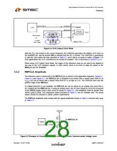
ULPI Output Clock
Mode
Table 5.10
Sourced by USB3320 at the CLKOUT pin
During start-up, the USB3320 monitors the CLKOUT pin to determine which mode has been
configured as described in Section 5.4.1.1.
The system must not drive voltage on the CLKOUT pin following POR or hardware reset that exceeds
the value of VIH_ED provided in Table 4.4.
5.4.1.1
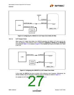
ULPI Input Clock Mode (60MHz REFCLK Mode)
When using ULPI Input Clock Mode, the Link must supply the 60MHz ULPI clock to the USB3320. As
shown in Figure 5.2, the 60MHz ULPI Clock is connected to the REFCLK pin, and the CLKOUT pin
is tied high to VDDIO. A simplified schematic using the ULPI Input Clock Mode is shown in Figure 8.2.
After the PLL has locked to the correct frequency, the USB3320 will de-assert DIR and the Link can
begin using the ULPI interface. The USB3320 is guaranteed to start the clock within the time specified
in Table 4.2. For Host applications, the ULPI AutoResume bit should be enabled. This is described in
Section 6.2.4.4.
REFSEL[2], REFSEL[1] and REFSEL[0] should all be tied to VDDIO for ULPI Input Clock Mode.
Revision 1.0 (07-14-09)
SMSC USB3320
DATA2S6HEET

 SMSC [ SMSC CORPORATION ]