Highly Integrated Full Featured Hi-Speed USB 2.0 ULPI Transceiver
Datasheet
Chapter 5 Architecture Overview
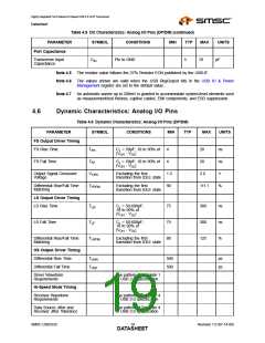
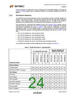
The USB3320 consists of the blocks shown in the diagram below. All pull-up resistors shown in this
diagram are connected internally to the VDD33 pin.
DrvVbus or’d with DrvVbusExternal
DATA7
VDD33
DATA6
IdGnd
DATA5
DATA4
DATA3
DATA2
DATA1
DATA0
STP
CPEN
ID
IdFloat
ULPI
Digitial
Rid Value
VDD33
VBUS
VBAT
VDD33
OVP
SessEnd
SessValid
VbusValid
NXT
DIR
CLKOUT
RESETB
LDO
VDDIO
VDD18
VDD33
REFCLK
XO
REFSEL0
REFSEL1
REFSEL2
Integrated
Low Jitter
PLL
HS/FS/LS
TX Encoding
TX
DP
DM
HS/FS/LS
RX Decoding
RX
BIAS
RBIAS
SPK_L
SPK_R
Figure 5.1 USB3320 Internal Block Diagram
5.1
ULPI Digital Operation and Interface
This section of the USB3320 is covered in detail in Chapter 6, ULPI Operation.
5.2
USB 2.0 Hi-Speed Transceiver
The blocks in the lower left-hand corner of Figure 5.1 interface to the DP/DM pins.
5.2.1
USB Transceiver
The USB3320 includes the receivers and transmitters that are compliant to the Universal Serial Bus
Specification Rev 2.0. The DP/DM signals in the USB cable connect directly to the receivers and
transmitters.
The RX block consists of a differential receiver for HS and separate receivers for FS/LS mode.
Depending on the mode, the selected receiver provides the serial data stream through the multiplexer
to the RX Logic block. For HS mode support, the HS RX block contains a squelch circuit to insure that
noise is not interpreted as data. The RX block also includes a single-ended receiver on each of the
data lines to determine the correct FS linestate.
Data from the TX Logic block is encoded, bit stuffed, serialized and transmitted onto the USB cable
by the TX block. Separate differential FS/LS and HS transmitters are included to support all modes.
The USB3320 TX block meets the HS signalling level requirements in the USB 2.0 Specification when
the PCB traces from the DP and DM pins to the USB connector have very little loss. In some systems,
SMSC USB3320
Revision 1.0 (07-14-09)
DATA2S3HEET

 SMSC [ SMSC CORPORATION ]