Highly Integrated Full Featured Hi-Speed USB 2.0 ULPI Transceiver
Datasheet
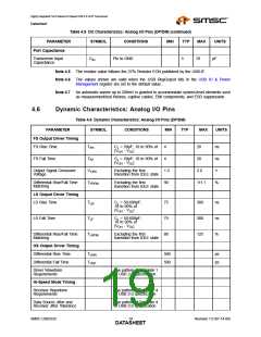
Table 4.5 DC Characteristics: Analog I/O Pins (DP/DM) (continued)
PARAMETER
SYMBOL
CONDITIONS
MIN
TYP
MAX
UNITS
Port Capacitance
Transceiver Input
Capacitance
CIN
Pin to GND
5
10
pF
Note 4.5 The resistor value follows the 27% Resistor ECN published by the USB-IF.
Note 4.6 The values shown are valid when the USB RegOutput bits in the USB IO & Power
Management register are set to the default value.
Note 4.7 An automatic waiver up to 200mV is granted to accommodate system-level elements such
as measurement/test fixtures, captive cables, EMI components, and ESD suppression.
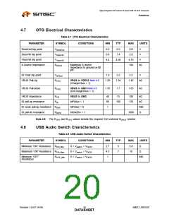
4.6
Dynamic Characteristics: Analog I/O Pins
Table 4.6 Dynamic Characteristics: Analog I/O Pins (DP/DM)
PARAMETER
SYMBOL
CONDITIONS
MIN
TYP
MAX
UNITS
FS Output Driver Timing
FS Rise Time
TFR
CL = 50pF; 10 to 90% of
4
20
ns
ns
V
|VOH - VOL
|
FS Fall Time
TFF
CL = 50pF; 10 to 90% of
|VOH - VOL
4
20
|
Output Signal Crossover
Voltage
VCRS
TFRFM
Excluding the first
transition from IDLE state
1.3
90
2.0
Differential Rise/Fall Time
Matching
Excluding the first
transition from IDLE state
111.1
%
LS Output Driver Timing
LS Rise Time
TLR
CL = 50-600pF;
10 to 90% of
75
75
80
300
300
125
ns
ns
%
|VOH - VOL
|
LS Fall Time
TLF
CL = 50-600pF;
10 to 90% of
|VOH - VOL
|
Differential Rise/Fall Time
Matching
TLRFM
Excluding the first
transition from IDLE state
HS Output Driver Timing
Differential Rise Time
Differential Fall Time
THSR
THSF
500
500
ps
ps
Driver Waveform
Requirements
Eye pattern of Template 1
in USB 2.0 specification
Hi-Speed Mode Timing
Receiver Waveform
Requirements
Eye pattern of Template 4
in USB 2.0 specification
Data Source Jitter and
Receiver Jitter Tolerance
Eye pattern of Template 4
in USB 2.0 specification
SMSC USB3320
Revision 1.0 (07-14-09)
DATA1S9HEET

 SMSC [ SMSC CORPORATION ]