Advanced I/O Controller with Motherboard GLUE Logic
Datasheet
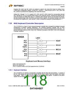
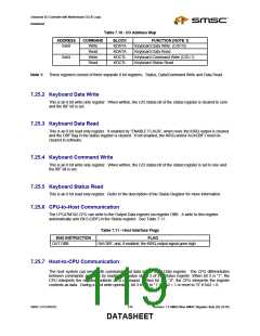
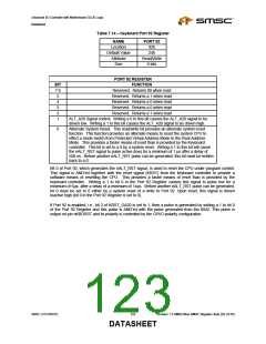
Table 7.10 - I/O Address Map
ADDRESS
COMMAND
Write
BLOCK
KDATA
KDATA
KDCTL
KDCTL
FUNCTION (NOTE 1)
Keyboard Data Write (C/D=0)
Keyboard Data Read
Keyboard Command Write (C/D=1)
Keyboard Status Read
0x60
Read
Write
Read
0x64
Note 1: These registers consist of three separate 8 bit registers. Status, Data/Command Write and Data Read.
7.25.2 Keyboard Data Write
This is an 8 bit write only register. When written, the C/D status bit of the status register is cleared to zero
and the IBF bit is set.
7.25.3 Keyboard Data Read
This is an 8 bit read only register. If enabled by “ENABLE FLAGS”, when read, the KIRQ output is cleared
and the OBF flag in the status register is cleared. If not enabled, the KIRQ and/or AUXOBF1 must be
cleared in software.
7.25.4 Keyboard Command Write
This is an 8 bit write only register. When written, the C/D status bit of the status register is set to one and
the IBF bit is set.
7.25.5 Keyboard Status Read
This is an 8 bit read only register. Refer to the description of the Status Register for more information.
7.25.6 CPU-to-Host Communication
The LPC47M182 CPU can write to the Output Data register via register DBB. A write to this register
automatically sets Bit 0 (OBF) in the Status register. See Table 7.11.
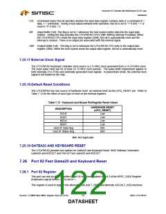
Table 7.11 - Host Interface Flags
8042 INSTRUCTION
OUT DBB
FLAG
Set OBF, and, if enabled, the KIRQ output signal goes high
7.25.7 Host-to-CPU Communication
The host system can send both commands and data to the Input Data register. The CPU differentiates
between commands and data by reading the value of Bit 3 of the Status register. When bit 3 is “1”, the
CPU interprets the register contents as a command. When bit 3 is “0”, the CPU interprets the register
contents as data. During a host write operation, bit 3 is set to “1” if SA2 = 1 or reset to “0” if SA2 = 0.
SMSC LPC47M182
119
Revision 1.8 SMSC/Non-SMSC Register Sets (02-24-05)
DATASHEET

 SMSC [ SMSC CORPORATION ]