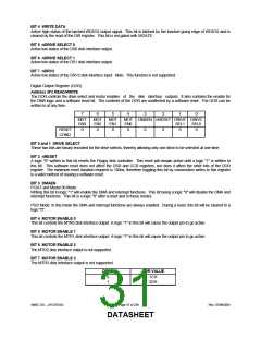
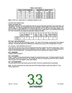
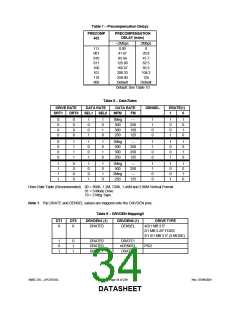
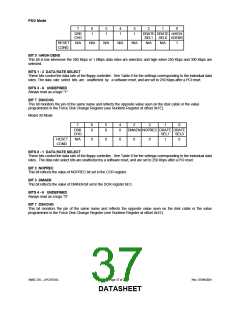
Table 6 − Drive Type ID
DIGITAL OUTPUT REGISTER REGISTER 3F3 - DRIVE TYPE ID
Bit 1
Bit 0
Bit 5
Bit 4
0
0
1
1
0
1
0
1
L0-CRF2 - B1
L0-CRF2 - B3
L0-CRF2 - B5
L0-CRF2 - B7
L0-CRF2 - B0
L0-CRF2 - B2
L0-CRF2 - B4
L0-CRF2 - B6
Note: L0-CRF2-Bx = Logical Device 0, Configuration Register F2, Bit x.
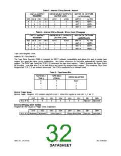
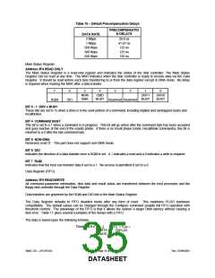
Data Rate Select Register (DSR)
Address 3F4 WRITE ONLY
This register is write only. It is used to program the data rate, amount of write precompensation, power down status, and
software reset. The data rate is programmed using the Configuration Control Register (CCR) not the DSR, for PC/AT
and PS/2 Model 30. Other applications can set the data rate in the DSR. The data rate of the floppy controller is the
most recent write of either the DSR or CCR. The DSR is unaffected by a software reset. A PCI reset will set the DSR to
02H, which corresponds to the default precompensation setting and 250 Kbps.
7
6
5
0
4
3
2
1
0
S/W
POWER
PRE-
PRE-
PRE-
DRATE DRATE
RESET DOWN
COMP2 COMP1 COMP0 SEL1
SEL0
RESET
COND.
0
0
0
0
0
0
1
0
BIT 0 and 1 DATA RATE SELECT
These bits control the data rate of the floppy controller. See Table 8 for the settings corresponding to the individual
data rates. The data rate select bits are unaffected by a software reset, and are set to 250 Kbps after a PCI reset.
BIT 2 through 4 PRECOMPENSATION SELECT
These three bits select the value of write precompensation that will be applied to the WDATA output signal. Table 7
shows the precompensation values for the combination of these bits settings. Track 0 is the default starting track
number to start precompensation. This starting track number can be changed by the configure command.
BIT 5 UNDEFINED
Should be written as a logic "0".
BIT 6 LOW POWER
A logic "1" written to this bit will put the floppy controller into manual low power mode. The floppy controller clock and
data separator circuits will be turned off. The controller will come out of manual low power mode after a software
reset or access to the Data Register or Main Status Register.
BIT 7 SOFTWARE RESET
This active high bit has the same function as the DOR RESET (DOR bit 2) except that this bit is self clearing.
Note: The DSR is Shadowed in the Floppy Data Rate Select Shadow Register, located at the offset 0x1F in the
runtime register block.
SMSC DS – LPC47S45x
Page 33 of 259
Rev. 07/09/2001
DATASHEET

 SMSC [ SMSC CORPORATION ]