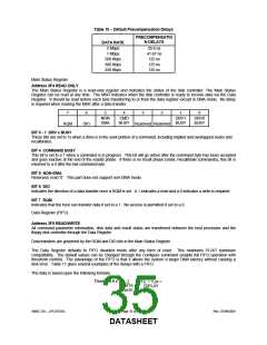
Table 10 − Default Precompensation Delays
PRECOMPENSATIO
N DELAYS
DATA RATE
2 Mbps
20.8 ns
41.67 ns
125 ns
125 ns
125 ns
1 Mbps
500 Kbps
300 Kbps
250 Kbps
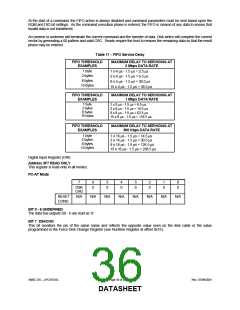
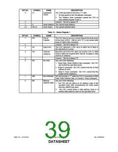
Main Status Register
Address 3F4 READ ONLY
The Main Status Register is a read-only register and indicates the status of the disk controller. The Main Status
Register can be read at any time. The MSR indicates when the disk controller is ready to receive data via the Data
Register. It should be read before each byte transferring to or from the data register except in DMA mode. No delay
is required when reading the MSR after a data transfer.
7
6
5
4
3
2
1
0
NON
DMA
CMD
BUSY
DRV1
BUSY
DRV0
BUSY
RQM
DIO
Reserved Reserved
BIT 0 - 1 DRV x BUSY
These bits are set to 1s when a drive is in the seek portion of a command, including implied and overlapped seeks and
recalibrates.
BIT 4 COMMAND BUSY
This bit is set to a 1 when a command is in progress. This bit will go active after the command byte has been accepted
and goes inactive at the end of the results phase. If there is no result phase (Seek, Recalibrate commands), this bit is
returned to a 0 after the last command byte.
BIT 5 NON-DMA
Reserved, read ‘0’. This part does not support non-DMA mode.
BIT 6 DIO
Indicates the direction of a data transfer once a RQM is set. A 1 indicates a read and a 0 indicates a write is required.
BIT 7 RQM
Indicates that the host can transfer data if set to a 1. No access is permitted if set to a 0.
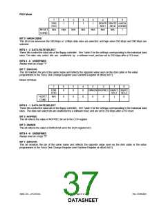
Data Register (FIFO)
Address 3F5 READ/WRITE
All command parameter information, disk data and result status are transferred between the host processor and the
floppy disk controller through the Data Register.
Data transfers are governed by the RQM and DIO bits in the Main Status Register.
The Data Register defaults to FIFO disabled mode after any form of reset. This maintains PC/AT hardware
compatibility. The default values can be changed through the Configure command (enable full FIFO operation with
threshold control). The advantage of the FIFO is that it allows the system a larger DMA latency without causing a
disk error. Table 11 gives several examples of the delays with a FIFO.
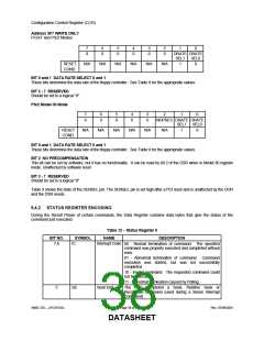
The data is based upon the following formula:
Threshold # x
1
x 8
- 1.5 μs =
DATA
RATE
DELAY
SMSC DS – LPC47S45x
Page 35 of 259
Rev. 07/09/2001
DATASHEET

 SMSC [ SMSC CORPORATION ]