At the start of a command, the FIFO action is always disabled and command parameters must be sent based upon the
RQM and DIO bit settings. As the command execution phase is entered, the FIFO is cleared of any data to ensure that
invalid data is not transferred.
An overrun or underrun will terminate the current command and the transfer of data. Disk writes will complete the current
sector by generating a 00 pattern and valid CRC. Reads require the host to remove the remaining data so that the result
phase may be entered.
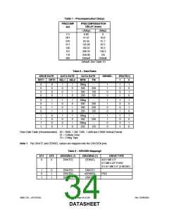
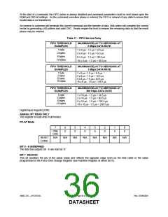
Table 11 − FIFO Service Delay
FIFO THRESHOLD
EXAMPLES
MAXIMUM DELAY TO SERVICING AT
2 Mbps DATA RATE
1 byte
2 bytes
8 bytes
15 bytes
1 x 4 μs - 1.5 μs = 2.5 μs
2 x 4 μs - 1.5 μs = 6.5 μs
8 x 4 μs - 1.5 μs = 30.5 μs
15 x 4 μs - 1.5 μs = 58.5 μs
FIFO THRESHOLD
EXAMPLES
MAXIMUM DELAY TO SERVICING AT
1 Mbps DATA RATE
1 byte
2 bytes
8 bytes
15 bytes
1 x 8 μs - 1.5 μs = 6.5 μs
2 x 8 μs - 1.5 μs = 14.5 μs
8 x 8 μs - 1.5 μs = 62.5 μs
15 x 8 μs - 1.5 μs = 118.5 μs
FIFO THRESHOLD
EXAMPLES
MAXIMUM DELAY TO SERVICING AT
500 Kbps DATA RATE
1 byte
2 bytes
8 bytes
15 bytes
1 x 16 μs - 1.5 μs = 14.5 μs
2 x 16 μs - 1.5 μs = 30.5 μs
8 x 16 μs - 1.5 μs = 126.5 μs
15 x 16 μs - 1.5 μs = 238.5 μs
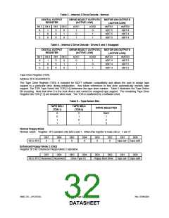
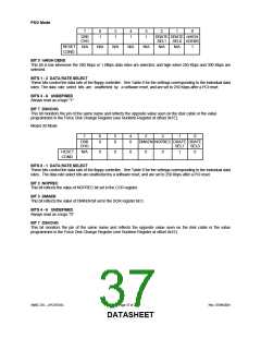
Digital Input Register (DIR)
Address 3F7 READ ONLY
This register is read-only in all modes.
PC-AT Mode
7
6
0
5
0
4
0
3
0
2
0
1
0
0
0
DSK
CHG
RESET
COND.
N/A
N/A
N/A
N/A
N/A
N/A
N/A
N/A
BIT 0 - 6 UNDEFINED
The data bus outputs D0 - 6 are read as ‘0’.
BIT 7 DSKCHG
This bit monitors the pin of the same name and reflects the opposite value seen on the disk cable or the value
programmed in the Force Disk Change Register (see Runtime Register at offset 0x1E).
SMSC DS – LPC47S45x
Page 36 of 259
Rev. 07/09/2001
DATASHEET

 SMSC [ SMSC CORPORATION ]