BIT 4 WRITE DATA
Active high status of the latched WDATA output signal. This bit is latched by the inactive going edge of WDATA and is
cleared by the read of the DIR register. This bit is not gated with WGATE.
BIT 5 nDRIVE SELECT 0
Active low status of the DS0 disk interface output.
BIT 6 nDRIVE SELECT 1
Active low status of the DS1 disk interface output.
BIT 7 nDRV2
Active low status of the DRV2 disk interface input. Note: This function is not supported.
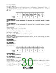
Digital Output Register (DOR)
Address 3F2 READ/WRITE
The DOR controls the drive select and motor enables of the disk interface outputs. It also contains the enable for
the DMA logic and a software reset bit. The contents of the DOR are unaffected by a software reset. The DOR can be
written to at any time.
7
6
5
4
3
2
1
0
MOT
EN3
MOT
EN2
MOT
EN1
MOT
EN0
DMAEN nRESET DRIVE DRIVE
SEL1
SEL0
RESET
COND.
0
0
0
0
0
0
0
0
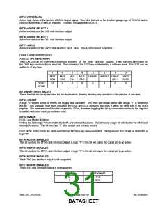
BIT 0 and 1 DRIVE SELECT
These two bits are binary encoded for the drive selects, thereby allowing only one drive to be selected at one time.
BIT 2 nRESET
A logic "0" written to this bit resets the Floppy disk controller. This reset will remain active until a logic "1" is written to
this bit. This software reset does not affect the DSR and CCR registers, nor does it affect the other bits of the DOR
register. The minimum reset duration required is 100ns, therefore toggling this bit by consecutive writes to this register
is a valid method of issuing a software reset.
BIT 3 DMAEN
PC/AT and Model 30 Mode:
Writing this bit to logic "1" will enable the DMA and interrupt functions. This bit being a logic "0" will disable the DMA and
interrupt functions. This bit is a logic "0" after a reset and in these modes.
PS/2 Mode: In this mode the DMA and interrupt functions are always enabled. During a reset, this bit will be cleared to a
logic "0".
BIT 4 MOTOR ENABLE 0
This bit controls the MTR0 disk interface output. A logic "1" in this bit will cause the output pin to go active.
BIT 5 MOTOR ENABLE 1
This bit controls the MTR1 disk interface output. A logic "1" in this bit will cause the output pin to go active.
BIT 6 MOTOR ENABLE 2
The MTR2 disk interface output is not supported.
BIT 7 MOTOR ENABLE 3
The MTR3 disk interface output is not supported.
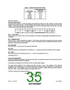
DRIVE
DOR VALUE
1CH
0
1
2DH
SMSC DS – LPC47S45x
Page 31 of 259
Rev. 07/09/2001
DATASHEET

 SMSC [ SMSC CORPORATION ]