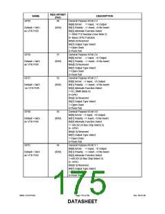
REG OFFSET
(hex)
NAME
DESCRIPTION
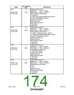
General Purpose I/0 bit 2.5
GP25
30
Bit[0] In/Out : =1 Input, =0 Output
Bit[1] Polarity : =1 Invert, =0 No Invert
Bit[2] Alternate Function Select
1= 8042 P12 function (User Note 2)
0= Basic GPIO Function
Bits[6:3] Reserved
Default = 0x01
on VTR POR
(R/W)
Bit[7] Output Type Select
1=Open Drain
0=Push Pull
GP26
31
General Purpose I/0 bit 2.6
Bit[0] In/Out : =1 Input, =0 Output
Bit[1] Polarity : =1 Invert, =0 No Invert
Bits[6:2] Reserved
Default = 0x01
on VTR POR
(R/W)
Bit[7] Output Type Select
1=Open Drain
0=Push Pull
GP27
32
General Purpose I/0 bit 2.7
Bit[0] In/Out : =1 Input, =0 Output
Bit[1] Polarity : =1 Invert, =0 No Invert
Bit[2] Alternate Function Select
1=IO_SMI# (Note 4)
Default = 0x01
on VTR POR
(R/W)
0=GPIO
Bits[6:3] Reserved
Bit[7] Output Type Select
1=Open Drain
0=Push Pull
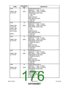
GP30
33
General Purpose I/0 bit 3.0
Bit[0] In/Out : =1 Input, =0 Output
Bit[1] Polarity :=1 Invert, =0 No Invert
Bit[2] Alternate Function Select
1= nXCS2 (X-Bus Chip Select 2)
0= GPIO
Default = 0x01
on VTR POR
(R/W)
Bits[6:3] Reserved
Bit[7] Output Type Select
1=Open Drain
0=Push Pull
GP31
34
General Purpose I/0 bit 3.1
Bit[0] In/Out : =1 Input, =0 Output
Bit[1] Polarity : =1 Invert, =0 No Invert
Bit[2] Alternate Function Select
1=nXCS3 (X-Bus Chip Select 3)
0= GPIO
Default = 0x01
on VTR POR
(R/W)
Bits[6:3] Reserved
Bit[7] Output Type Select
1=Open Drain
0=Push Pull
SMSC LPC47S45x
Page 175 of 259
Rev. 06-01-06
DATASHEET

 SMSC [ SMSC CORPORATION ]