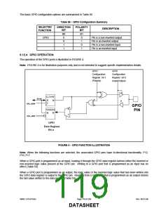
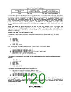
Table 59 − GPIO Read/Write Behavior
HOST OPERATION
GPIO INPUT PORT
GPIO OUTPUT PORT
Read
Write
Latched Value Of Gpio Pin
No Effect
Last Write To GPIO Data Register
Bit Placed In GPIO Data Register
The LPC47S45x provides 37 GPIOs that can directly generate a PME. See the table in the next section. The polarity
bit in the GPIO control registers select the edge on these GPIO pins that will set the associated status bit in the
PME_STS2 – PME_STS7 registers. The default is the low-to-high edge. If the corresponding enable bit in the
PME_EN 2 – PME_EN7 registers and the PME_EN bit in the PME_EN register is set, a PME will be generated.
These registers are located in the Runtime Registers Block, which are located at the address contained in the
configuration registers 0x60 and 0x61 in Logical Device A. The PME status bits for the GPIOs are cleared on a write
of ‘1’. In addition, the LPC47S45x provides 36 GPIOs that can directly generate an SMI. See the table in the next
section.
Note: PME events can also be generated by the PM1 and GPE status registers. GP23, GP34, GP35, and
GP[50:57] can generate a PME event if they are enabled in either the PME enable registers or the GPE enable
registers. See section 7 ACPI/PME/SMI Features on page 147 for a detailed description of the ACPI specific
registers, PM1 and GPE.
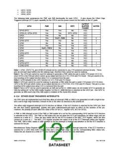
6.12.5 GPIO PME AND SMI FUNCTIONALITY
The following GPIOs are dedicated wakeup GPIOs with a status and enable bit in the PME status and enable
registers:
GP10-GP17
GP20-GP27
GP30-GP37
GP41, GP43
GP50-GP57
GP60, GP61, GP62
This following is the list of PME status and enable registers for their corresponding GPIOs:
PME_STS2 and PME_EN2 for GP10-GP17
PME_STS3 and PME_EN3 for GP20-GP27
PME_STS4 and PME_EN4 for GP30-GP33, GP41, GP43, GP60, GP61
PME_STS5 and PME_EN5 for GP50-GP57
PME_STS7 and PME_EN7 for GP34-GP37, GP62
The following GPIOs can directly generate an SMI and have a status and enable bit in the SMI status and enable
registers.
GP10-GP17
GP20-22, GP24-27
GP30-GP37
GP41, GP43
GP50-GP57
GP60, GP61, GP62
The following SMI status and enable registers for these GPIOs:
SMI_STS3 and SMI_EN3 for GP20-22, GP24-27, GP60
SMI_STS4 and SMI_EN4 for GP30-GP33, GP41, GP43, GP61
SMI_STS5 and SMI_EN5 for GP50-GP57
SMI_STS5 and SMI_EN5 for GP10-GP17
SMI_STS7 and SMI_EN7 for GP34-GP37, GP62
The following GPIOs have “either edge triggered interrupt” (EETI) input capability. These GPIOs can generate a
PME and an SMI on both a high-to-low and a low-to-high edge on the GPIO pin. These GPIOs have a status bit in
the MSC_STS status register that is set on both edges. The corresponding bits in the PME and SMI status registers
are also set on both edges.
SMSC LPC47S45x
Page 120 of 259
Rev. 06-01-06
DATASHEET

 SMSC [ SMSC CORPORATION ]