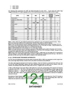
GP21, GP22
GP41, GP43
GP60, GP61
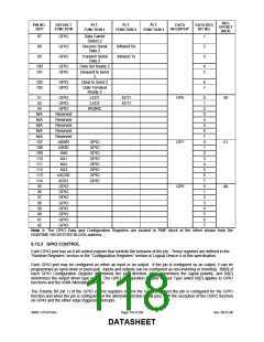
The following table summarizes the PME and SMI functionality for each GPIO. It also shows the Either Edge
Triggered Interrupt (EETI) input capability for the GPIOs and the power source for the buffer on the I/O pads.
OUTPUT
GPIO
GP10-GP17
PME
SMI
EETI
BUFFER
POWER
NOTES
Yes
Yes
Yes
Yes
No
GP21-GP22
No
VCC
VCC
VCC
VCC
VCC
VCC
VCC
VTR
VCC
VCC
VCC
VCC
VCC
VCC
VCC
GP20-22, GP24-GP26
GP23
Yes
No
GP27
Yes
Yes/IO_SMI#
Yes
No
5
2
1
GP30-GP37
GP40
Yes
No
No
No
No
GP41
Yes
Yes
Yes
No
GP42
No/IO_PME#
Yes
No
GP43
Yes
Yes
No
3
4
GP50-GP57
GP60
Yes
Yes
Yes
Yes
Yes
Yes
No
GP61
Yes
Yes
GP62
Yes
Yes
GP70-GP77
GP80-GP87
No
No
No
1
1
No
No
No
Note 1: GP40, GP[70:77], and GP[80:87] should not be connected to any VTR powered external circuitry. These
pins do not have input buffers into the wakeup logic, therefore they cannot be used for wakeup.
Note 2: The GP33 pin cannot be used for wakeup to generate a PME while the part is under VTR power (VCC=0)
since GP33 is the FAN pin which comes up as output and low on a VCC POR and PCI Reset. This pin reverts to its
non-inverting GPIO output function when VCC is removed from the part.
Note 3: GP43 defaults to the GPIO function on VCC POR and PCI Reset.
Note 4: GP53 pin cannot be used for wakeup to generate a PME while the part is under VTR power (VCC=0) since
GP53 is the IRTX pin which comes up as output and low on a VTR POR, VCC POR and PCI Reset. This pin is a non-
inverting GPIO output (low) when VCC is removed from the part.
Note 5: Since GP27 can be used to generate an SMI and as the IO_SMI# output, do not enable GP27 to generate an
SMI (by setting bit 7 of the SMI Enable Register 3) if the IO_SMI# function is selected on the GP27 pin. Use GP27 to
generate an SMI event only if the SMI output is enabled on the Serial IRQ stream.
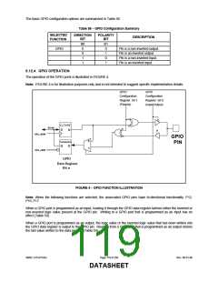
6.12.6 EITHER EDGE TRIGGERED INTERRUPTS
Six GPIO pins are implemented such that they allow an interrupt (PME or SMI) to be generated on both a high-to-low
and a low-to-high edge transition, instead of one or the other as selected by the polarity bit.
The either edge triggered interrupts (EETI) function as follows: If the EETI function is selected for the GPIO pin, then
the bits that control input/output, polarity and open collector/push-pull have no effect on the function of the pin.
However, the polarity bit does affect the value of the GP bit (i.e., register GP2, bit 2 for GP22).
A PME or SMI interrupt occurs if the PME or SMI enable bit is set for the corresponding GPIO and the EETI function
is selected on the GPIO. The PME or SMI status bits are set when the EETI pin transitions (on either edge) and are
cleared on a write of ‘1’. There are also status bits for the EETIs located in the MSC_STS register, which are also
cleared on a write of ‘1’. The MSC_STS register provides the status of all of the EETI interrupts within one register.
The PME, SMI or MSC status is valid whether or not the interrupt is enabled and whether or not the EETI function is
selected for the pin.
Miscellaneous Status Register (MSC_STS) is for the either edge triggered interrupt status bits. If the EETI function is
selected for a GPIO then both a high-to-low and a low-to-high edge will set the corresponding MSC status bits.
Status bits are cleared on a write of ‘1’. See Runtime Register section for more information.
SMSC LPC47S45x
Page 121 of 259
Rev. 06-01-06
DATASHEET

 SMSC [ SMSC CORPORATION ]