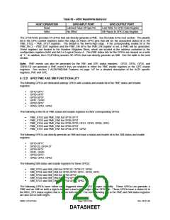
The basic GPIO configuration options are summarized in Table 58.
Table 58 − GPIO Configuration Summary
SELECTED
FUNCTION
DIRECTION
BIT
POLARITY
BIT
DESCRIPTION
B0
0
B1
0
GPIO
Pin is a non-inverted output.
Pin is an inverted output.
Pin is a non-inverted input.
Pin is an inverted input.
0
1
1
0
1
1
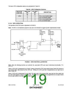
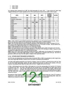
6.12.4 GPIO OPERATION
The operation of the GPIO ports is illustrated in FIGURE 4.
Note: FIGURE 4 is for illustration purposes only and in not intended to suggest specific implementation details.
GPIO
GPIO
Configuration
Register bit-1
(Polarity)
Configuration
Register bit-0
(Input/Output)
D-TYPE
SD-bit
D
Q
GPx_nIOW
GPx_nIOR
GPIO
PIN
0
1
Transparent
Q
D
GPIO
Data Register
Bit-n
FIGURE 4 − GPIO FUNCTION ILLUSTRATION
Note: When the following functions are selected, the associated GPIO pins have bi-directional functionality: P12,
P16, P17.
When a GPIO port is programmed as an input, reading it through the GPIO data register latches either the inverted or
non-inverted logic value present at the GPIO pin. Writing to a GPIO port that is programmed as an input has no
effect (Table 59).
When a GPIO port is programmed as an output, the logic value or the inverted logic value that has been written into
the GPIO data register is output to the GPIO pin. Reading from a GPIO port that is programmed as an output returns
the last value written to the data register (Table 59).
SMSC LPC47S45x
Page 119 of 259
Rev. 06-01-06
DATASHEET

 SMSC [ SMSC CORPORATION ]