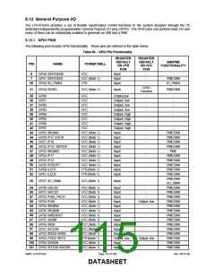
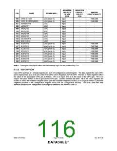
REG
OFFSET
(HEX)
ALT.
ALT.
ALT.
PIN NO.
/QFP
DEFAULT
FUNCTION
DATA
DATA REG
BIT NO.
REGISTER1
FUNCTION 1
FUNCTION 2
FUNCTION 3
97
98
99
GPIO
GPIO
GPIO
Data Carrier
Detect 2
1
2
3
Receive Serial
Data 2
Infrared Rx
Infrared Tx
Transmit Serial
Data 2
100
101
GPIO
GPIO
Data Set Ready 2
4
5
Request to Send
2
102
103
GPIO
GPIO
Clear to Send 2
6
7
Date Terminal
Ready 2
51
52
GPIO
GPIO
LED1
LED2
EETI
EETI
GP6
GP7
GP8
0
1
2
3
4
5
6
7
0
1
2
3
4
5
6
7
0
1
2
3
4
5
6
7
50
51
4A
43
GPIO
IRQINC
N/A
N/A
N/A
N/A
N/A
107
108
109
110
111
112
113
114
35
Reserved
Reserved
Reserved
Reserved
Reserved
nXWR
nXRD
XA0
GPIO
GPIO
GPIO
GPIO
GPIO
GPIO
GPIO
GPIO
XA1
XA2
XA3
nXCS0
XCS1
GPIO
36
GPIO
37
GPIO
38
GPIO
39
GPIO
40
GPIO
41
GPIO
42
GPIO
Note 1: The GPIO Data and Configuration Registers are located in PME block at the offset shown from the
RUNTIME REGISTERS BLOCK address.
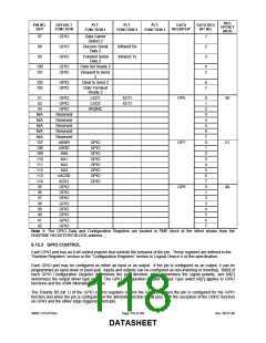
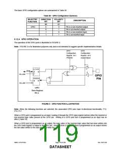
6.12.3 GPIO CONTROL
Each GPIO port has an 8-bit control register that controls the behavior of the pin. These registers are defined in the
“Runtime Registers” section or the “Configuration Registers” section in Logical Device A of this specification.
Each GPIO port may be configured as either an input or an output. If the pin is configured as an output, it can be
programmed as open-drain or push-pull. Inputs and outputs can be configured as non-inverting or inverting. Bit[0] of
each GPIO Configuration Register determines the port direction, bit[1] determines the signal polarity, and bit[7]
determines the output driver type select. The GPIO configuration register Output Type select bit[7] applies to GPIO
functions and the nSMI Alternate functions.
The Polarity Bit (bit 1) of the GPIO control registers control the GPIO pin when the pin is configured for the GPIO
function and when the pin is configured for the alternate function for all pins, with the exception of the DDRC function
on GP43 and the either edge triggered interrupts.
SMSC LPC47S45x
Page 118 of 259
Rev. 06-01-06
DATASHEET

 SMSC [ SMSC CORPORATION ]