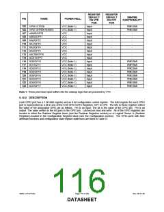
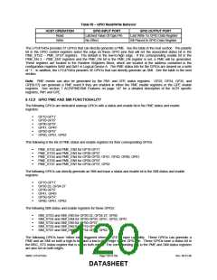
REGISTER
DEFAULT
ON VTR
POR
REGISTER
DEFAULT
ON VCC
POR
SMI/PME
FUNCTIONALITY
PIN
NAME
POWER WELL
102 GP56 /CTS2#
103 GP57 /DTR2# /SADR1
107 nXWR/GP70
108 nXRD/GP71
109 XA0/GP72
110 XA1/GP73
111 XA2/GP74
112 XA3/GP75
113 nXCS0/GP76
114 XCS1/GP77
116 XD0/GP10
117 XD1/GP11
118 XD2/GP12
119 XD3/GP13
120 XD4/GP14
121 XD5/GP15
122 XD6/GP16
123 XD7/GP17
VCC (Note 1)
VCC (Note 1)
VCC
Input
-
-
-
-
-
-
-
-
-
-
-
-
-
-
-
-
-
-
PME/SMI
Input
Input
Input
Input
Input
Input
Input
Input
Input
Input
Input
Input
Input
Input
Input
Input
Input
PME/SMI
-
VCC
-
VCC
-
VCC
-
VCC
-
VCC
-
VCC
-
VCC
-
VCC (Note 1)
VCC (Note 1)
VCC (Note 1)
VCC (Note 1)
VCC (Note 1)
VCC (Note 1)
VCC (Note 1)
VCC (Note 1)
PME/SMI
PME/SMI
PME/SMI
PME/SMI
PME/SMI
PME/SMI
PME/SMI
PME/SMI
Note 1: These pins have input buffers into the wakeup logic that are powered by VTR.
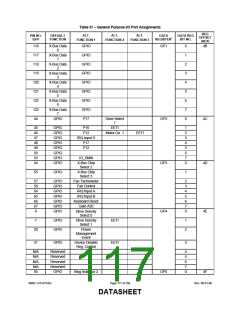
6.12.2 DESCRIPTION
Each GPIO port has a 1-bit data register and an 8-bit configuration control register. The data register for each GPIO
port is represented as a bit in one of the 8-bit GPIO DATA Registers, GP1 to GP8. The bits in these registers reflect
the value of the associated GPIO pin as follows. Pin is an input: The bit is the value of the GPIO pin. Pin is an
output: The value written to the bit goes to the GPIO pin. Latched on read and write. All of the GPIO registers are
located in either the Runtime Register block (see the Runtime Registers section) or in Logical Device A (Runtime
Registers) located in the Configuration Register block (see the Configuration section). The GPIO ports with their
alternate functions and configuration state register addresses are listed in Table 57.
SMSC LPC47S45x
Page 116 of 259
Rev. 06-01-06
DATASHEET

 SMSC [ SMSC CORPORATION ]