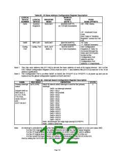
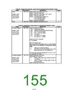
DEVICE ON (ACTIVE) = (Activate Bit SET or Pwr/Control Bit SET).
The Logical device's Activate Bit and its Pwr/Control Bit are linked such that setting or clearing one sets or
clears the other.
Note 2: If the I/O Base Addr of the logical device is not within the Base I/O range as shown in the Logical Device I/O
map, then read or write is not valid and is ignored.
Note 3: The default value of the Primary Interrupt Select register for logical device 0 is 0x06.
Note 4: The default value of the DMA Channel Select register for logical device 0 (FDD) is 0x02 and for logical device
3 and 5 is 0x04.
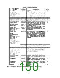
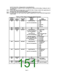
Table 65 - I/O Base Address Configuration Register Description
LOGICAL
DEVICE
NUMBER
0x00
BASE I/O
RANGE
(NOTE 1)
LOGICAL
DEVICE
FDC
REGISTER
INDEX
0x60,0x61
FIXED
BASE OFFSETS
[0x0100:0x0FF8]
+0 : SRA
+1 : SRB
ON 8 BYTE BOUNDARIES +2 : DOR
+3 : TSR
+4 : MSR/DSR
+5 : FIFO
+7 : DIR/CCR
n/a
0x01
0x02
0x03
Reserved
Reserved
Parallel
Port
n/a
n/a
0x60,0x61
n/a
n/a
n/a
[0x0100:0x0FFC]
+0 : Data/ecpAfifo
ON 4 BYTE BOUNDARIES +1 : Status
(EPP Not supported)
or
+2 : Control
+400h :
[0x0100:0x0FF8]
cfifo/ecpDfifo/tfifo/cnfgA
ON 8 BYTE BOUNDARIES +401h : cnfgB
+402h : ecr
(all modes supported,
+3 : EPP Address
EPP is only available when +4 : EPP Data 0
the base address is on an 8- +5 : EPP Data 1
byte boundary)
+6 : EPP Data 2
+7 : EPP Data 3
+0 : RB/TB/LSB div
+1 : IER/MSB div
0x04
0x05
Serial Port 1
0x60,0x61
0x60,0x61
[0x0100:0x0FF8]
ON 8 BYTE BOUNDARIES +2 : IIR/FCR
+3 : LCR
+4 : MSR
+5 : LSR
+6 : MSR
+7 : SCR
Serial Port 2
[0x0100:0x0FF8]
+0 : RB/TB/LSB div
+1 : IER/MSB div
ON 8 BYTE BOUNDARIES +2 : IIR/FCR
+3 : LCR
+4 : MSR
+5 : LSR
+6 : MSR
+7 : SCR
0x06
0x07
Reserved
KYBD
n/a
n/a
n/a
n/a
Not Relocatable
+0 : Data Register
Fixed Base Address: 60,64 +4 : Command/Status
Reg.
0x08
0x09
Reserved
Game Port
n/a
0x60,0x61
n/a
n/a
[0x0100:0x0FFF]
on 1 byte boundaries
+00: Game Port Register
Page 151

 SMSC [ SMSC CORPORATION ]