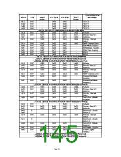
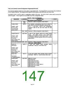
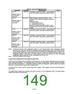
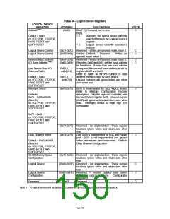
Chip Level (Global) Control/Configuration Registers[0x00-0x2F]
The chip-level (global) registers lie in the address range [0x00-0x2F]. The design MUST use all 8 bits of the ADDRESS
Port for register selection. All unimplemented registers and bits ignore writes and return zero when read.
The INDEX PORT is used to select a configuration register in the chip. The DATA PORT is then used to access the
selected register. These registers are accessible only in the Configuration Mode.
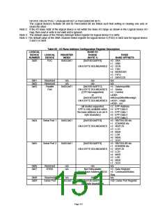
Table 63 - Chip Level Registers
REGISTER
ADDRESS
DESCRIPTION
Chip (Global) Control Registers
STATE
0x00 -
0x01
Reserved - Writes are ignored, reads return 0.
Config Control
0x02 W
The hardware automatically clears this bit after the
write, there is no need for software to clear the bits.
Bit 0 = 1: Soft Reset. Refer to the "Configuration
Registers" table for the soft reset value for each
register.
C
Default = 0x00
on VCC POR,
VTR POR and
HARD RESET
0x03 - 0x06 Reserved - Writes are ignored, reads return 0.
Logical Device #
0x07 R/W A write to this register selects the current logical
device. This allows access to the control and
configuration registers for each logical device. Note:
The Activate command operates only on the selected
logical device.
C
Default = 0x00
on VCC POR,
VTR POR,
SOFT RESET and
HARD RESET
Card Level Reserved 0x08 - 0x1F Reserved - Writes are ignored, reads return 0.
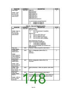
Chip Level, SMSC Defined
Device ID -
Hard wired
0x20 R
A
read only register which provides device
C
identification. Bits[7:0] = 0x59 when read.
Default = 0x59
on VCC POR,
VTR POR,
SOFT RESET and
HARD RESET
Device Rev
0x21 R
A read only register which provides device revision
information. Bits[7:0] = current revision when read.
C
C
Hard wired
= Current Revision
PowerControl
0x22 R/W Bit[0] FDC Power
Bit[1] Reserved
Default = 0x00
on VCC POR,
VTR POR,
SOFT RESET and
HARD RESET
Bit[2] Game Port Power
Bit[3] Parallel Port Power
Bit[4] Serial Port 1 Power
Bit[5] Serial Port 2 Power (Note 2)
Bit[6] Serial Port 3 Power
Bit[7] Reserved
Page 147

 SMSC [ SMSC CORPORATION ]