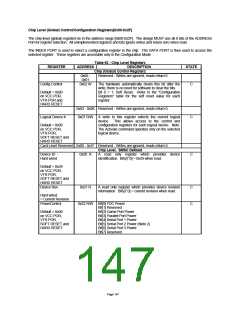
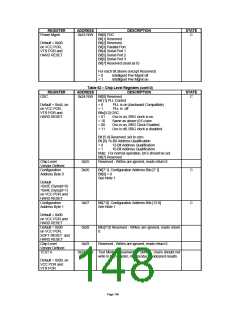
REGISTER
Power Mgmt
ADDRESS
0x23 R/W Bit[0] FDC
DESCRIPTION
STATE
C
Bit[1] Reserved
Default = 0x00
on VCC POR,
VTR POR and
HARD RESET
Bit[2] Reserved
Bit[3] Parallel Port
Bit[4] Serial Port 1
Bit[5] Serial Port 2
Bit[6] Serial Port 3
Bit[7] Reserved (read as 0)
For each bit above (except Reserved)
= 0
= 1
Intelligent Pwr Mgmt off
Intelligent Pwr Mgmt on
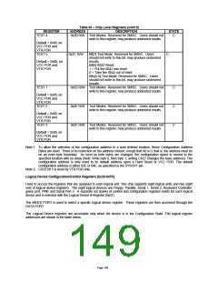
Table 63 – Chip Level Registers (cont’d)
ADDRESS DESCRIPTION
REGISTER
STATE
OSC
0x24 R/W Bit[0] Reserved
Bit [1] PLL Control
C
Default = 0x44, on
on VCC POR,
VTR POR and
HARD RESET
= 0
= 1
PLL is on (backward Compatible)
PLL is off
Bits[3:2] OSC
= 01
= 10
= 00
= 11
Osc is on, BRG clock is on.
Same as above (01) case.
Osc is on, BRG Clock Enabled.
Osc is off, BRG clock is disabled.
Bit [5:4] Reserved, set to zero
Bit [6] 16-Bit Address Qualification
= 0
= 1
12-Bit Address Qualification
16-Bit Address Qualification
Note: For normal operation, bit 6 should be set.
Bit[7] Reserved
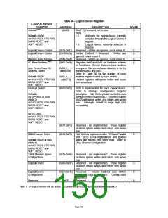
Chip Level
0x25
0x26
Reserved - Writes are ignored, reads return 0.
Vendor Defined
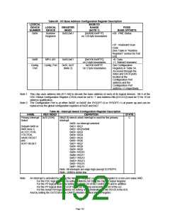
Configuration
Address Byte 0
Bit[7:1] Configuration Address Bits [7:1]
Bit[0] = 0
C
C
See Note 1
Default
=0x2E (Sysopt=0)
=0x4E (Sysopt=1)
on VCC POR and
HARD RESET
Configuration
0x27
Bit[7:0] Configuration Address Bits [15:8]
See Note 1
Address Byte 1
Default = 0x00
on VCC POR and
HARD RESET
Default = 0x00
on VCC POR,
SOFT RESET and
HARD RESET
Chip Level
0x28
0x29
Bits[7:0] Reserved - Writes are ignored, reads return
0.
Reserved - Writes are ignored, reads return 0.
Vendor Defined
TEST 6
0x2A R/W Test Modes: Reserved for SMSC. Users should not
write to this register, may produce undesired results.
Default = 0x00, on
VCC POR and
VTR POR
Page 148

 SMSC [ SMSC CORPORATION ]