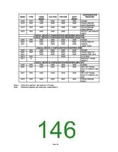
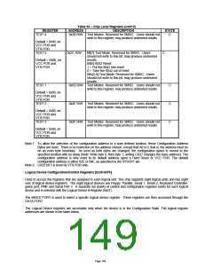
Table 63 – Chip Level Registers (cont’d)
REGISTER
TEST 4
ADDRESS
DESCRIPTION
STATE
0x2B R/W Test Modes: Reserved for SMSC. Users should not
write to this register, may produce undesired results.
C
Default = 0x00, on
VCC POR and
VTR POR
TEST 5
0x2C R/W
Bit[7] Test Mode: Reserved for SMSC. Users
should not write to this bit, may produce undesired
results.
Bit[6] 8042 Reset:
1 = Put the 8042 into reset
C
Default = 0x00, on
VCC POR and
VTR POR
0 = Take the 8042 out of reset
Bits[5:0] Test Mode: Reserved for SMSC. Users
should not write to this bit, may produce undesired
results.
TEST 1
0x2D R/W Test Modes: Reserved for SMSC. Users should not
write to this register, may produce undesired results.
C
C
C
Default = 0x00, on
VCC POR and
VTR POR
TEST 2
0x2E R/W Test Modes: Reserved for SMSC. Users should not
write to this register, may produce undesired results.
Default = 0x00, on
VCC POR and
VTR POR
TEST 3
0x2F R/W Test Modes: Reserved for SMSC. Users should not
write to this register, may produce undesired results.
Default = 0x00, on
VCC POR and
VTR POR
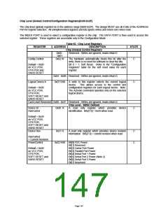
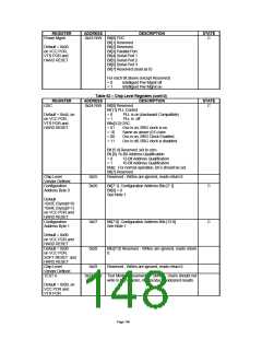
Note 1: To allow the selection of the configuration address to a user defined location, these Configuration Address
Bytes are used. There is no restriction on the address chosen, except that A0 is 0, that is, the address must be
on an even byte boundary. As soon as both bytes are changed, the configuration space is moved to the
specified location with no delay (Note: Write byte 0, then byte 1; writing CR27 changes the base address). The
configuration address is only reset to its default address upon a Hard Reset or VCC POR. The default
configuration address is either 02E or 04E, as specified by the SYSOPT pin.
Note 2: CR22 bit 5 is reset by VTR POR only.
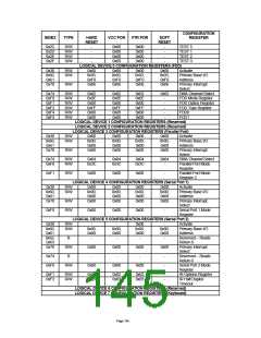
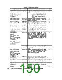
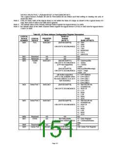
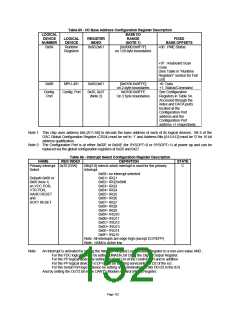
Logical Device Configuration/Control Registers [0x30-0xFF]
Used to access the registers that are assigned to each logical unit. This chip supports eight logical units and has eight
sets of logical device registers. The eight logical devices are Floppy, Parallel, Serial 1, Serial 2, Keyboard Controller,
game port, PME and Serial Port 3. A separate set (bank) of control and configuration registers exists for each logical
device and is selected with the Logical Device # Register (0x07).
The INDEX PORT is used to select a specific logical device register. These registers are then accessed through the
DATA PORT.
The Logical Device registers are accessible only when the device is in the Configuration State. The logical register
addresses are shown in the table below.
Page 149

 SMSC [ SMSC CORPORATION ]