REG OFFSET
NAME
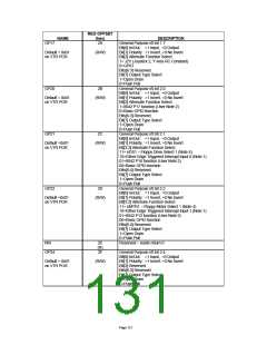
SMI_EN5
(hex)
1A
DESCRIPTION
SMI Enable Register 5
This register is used to enable the different interrupt sources
Default = 0x00
on VTR POR
(R/W)
onto the group nSMI output.
1=Enable
0=Disable
Bit[0] GP54
Bit[1] GP55
Bit[2] GP56
Bit[3] GP57
Bit[4] Reserved
Bit[5] Reserved
Bit[6] FAN_TACH1
Bit[7] FAN_TACH2
Reserved – reads return 0
N/A
1B
(R)
1C
MSC_STS
Miscellaneous Status Register
Bits[5:0] can be cleared by writing a 1 to their position
(writing a 0 has no effect).
Default = 0x00
on VTR POR
(R/W)
Bit[0] Either Edge Triggered Interrupt Input 0 Status. This
bit is set when an edge occurs on the GP21 pin.
Bit[1] Either Edge Triggered Interrupt Input 1 Status. This
bit is set when an edge occurs on the GP22 pin.
Bit[2] Either Edge Triggered Interrupt Input 2 Status. This
bit is set when an edge occurs on the GP41 pin.
Bit[3] Either Edge Triggered Interrupt Input 3 Status. This
bit is set when an edge occurs on the GP43 pin.
Bit[4] Either Edge Triggered Interrupt Input 4 Status. This
bit is set when an edge occurs on the GP60 pin.
Bit[5] Either Edge Triggered Interrupt Input 5 Status. This
bit is set when an edge occurs on the GP61 pin.
Bit[7:6] Reserved. This bit always returns zero.
Reserved – reads return 0
N/A
1D
(R)
1E
Force Disk Change
Force Disk Change
Bit[0] Force Disk Change for FDC0
0=Inactive
Default = 0x01 on
VCC POR
(R/W)
1=Active
Bit[1] Force Disk Change for FDC1
0=Inactive
1=Active
Force Change 0 and 1 can be written to 1 but are not
clearable by software.
Force Change 0 is cleared on nSTEP and nDS0
Force Change 1 is cleared on nSTEP and nDS1
DSKCHG (FDC DIR Register, Bit 7) = (nDS0 AND Force
Change 0) OR (nDS1 AND Force Change 1) OR nDSKCHG
Setting either of the Force Disk Change bits active ‘1’ forces
the FDD nDSKCHG input active when the appropriate drive
has been selected.
Bit[7:2] Reserved
Page 127

 SMSC [ SMSC CORPORATION ]