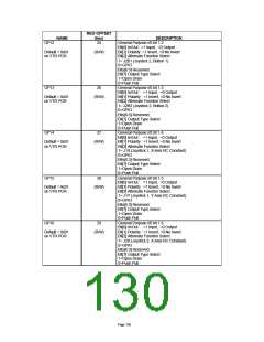
REG OFFSET
NAME
SMI_EN1
(hex)
16
DESCRIPTION
SMI Enable Register 1
This register is used to enable the different interrupt sources
onto the group nSMI output.
1=Enable
Default = 0x00
on VTR POR
(R/W)
0=Disable
Bit[0] Reserved
Bit[1] EN_PINT
Bit[2] EN_U2INT
Bit[3] EN_U1INT
Bit[4] EN_FINT
Bit[5] EN_MPU-401 INT
Bit[6] Reserved
Bit[7] Reserved (Note 7)
SMI_EN2
17
SMI Enable Register 2
This register is used to enable the different interrupt sources
onto the group nSMI output, and the group nSMI output onto
the nIO_SMI GPI/O pin, the serial IRQ stream or into the
PME Logic.
Default = 0x00
on VTR POR
(R/W)
Unless otherwise noted,
1=Enable
0=Disable
Bit[0] EN_MINT
Bit[1] EN_KINT
Bit[2] EN_IRINT
Bit[3] Reserved
Bit[4] EN_P12
Bit[5] EN_SMI_PME (Enable group SMI into PME logic)
Bit[6] EN_SMI_S (Enable group SMI onto serial IRQ)
Bit[7] EN_SMI (Enable group SMI onto nIO_SMI pin)
SMI_EN3
18
SMI Enable Register 3
This register is used to enable the different interrupt sources
Default = 0x00
on VTR POR
(R/W)
onto the group nSMI output.
1=Enable
0=Disable
Bit[0] GP20
Bit[1] GP21
Bit[2] GP22
Bit[3] Reserved
Bit[4] GP24
Bit[5] GP25
Bit[6] GP26
Bit[7] GP60
SMI_EN4
19
SMI Enable Register 4
This register is used to enable the different interrupt sources
Default = 0x00
on VTR POR
(R/W)
onto the group nSMI output.
1=Enable
0=Disable
Bit[0] GP30
Bit[1] GP31
Bit[2] GP32
Bit[3] GP33
Bit[4] GP41
Bit[5] GP42
Bit[6] GP43
Bit[7] GP61
Page 126

 SMSC [ SMSC CORPORATION ]