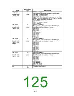
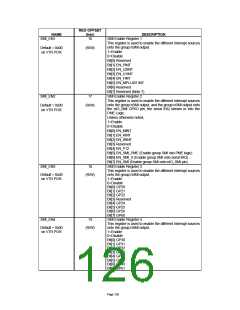
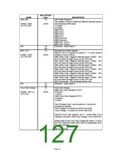
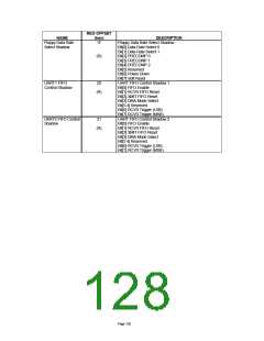
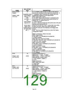
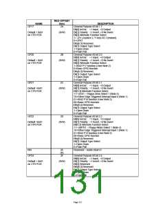
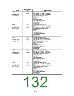
REG OFFSET
NAME
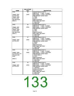
Device Disable
Register
(hex)
22
DESCRIPTION
If “0” (enabled), bits[7:3] have no effect on the devices;
devices are controlled by their respective activate bits. If
Read/Write when “1” (disabled), bits[7:3] override the activate bits in the
Default = 0x00
VTR POR
GP43 register
bits[3:2] = 01
AND
GP43 pin = 0
OR
configuration registers for each logical block.
Bit[0]: Floppy Write Protect.
0= no effect: floppy write protection is controlled by the
write protect pin or the forced write protect bit (bit 0 of
register 0xF1 in Logical Device 0);
GP43 register
1= Write Protected.
If set to 1, this bit overrides the write protect pin on the part
and the forced write protect bit.
bits[3:2] ≠ 01
nWRTPRT (to the FDC Core) = (nDS0 AND Force Write
Protect) OR (nDS1 AND Force Write Protect)OR
nWRTPRT (from the FDD Interface) OR Floppy Write
Protect
Note: The Force Write Protect bit is in the FDD Option
configuration register.
READ-ONLY
When GP43
register bits[3:2]
=01 AND GP43
pin = 1
Bits[2:1]: Reserved. Return 0 on read.
Bit[3]: Floppy Enable.
0=No effect: FDC controlled by its activate bit;
1=Floppy Disabled
Bit[4]: MPU-401 Serial Port Enable.
0=No effect: MPU-401 UART controlled by its activate bit;
1=MPU-401 UART Disabled
Bit[5]: Serial Port 2 Enable.
0=No effect: UART2 controlled by its activate bit;
1=UART2 Disabled
Bit[6]: Serial Port 1 Enable.
0=No effect: UART1 controlled by its activate bit;
1=UART1 Disabled
Bit[7]: Parallel Port Enable.
0=No effect: PP controlled by its activate bit;
1=PP Disabled
GP10
23
General Purpose I/0 bit 1.0
Bit[0] In/Out : =1 Input, =0 Output
Bit[1] Polarity : =1 Invert, =0 No Invert
Bit[2] Alternate Function Select
1=J1B1 (Joystick 1, Button 1)
0=GPIO
Default = 0x01
on VTR POR
(R/W)
Bits[6:3] Reserved
Bit[7] Output Type Select
1=Open Drain
0=Push Pull
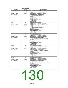
GP11
Default = 0x01
on VTR POR
24
General Purpose I/0 bit 1.1
Bit[0] In/Out : =1 Input, =0 Output
Bit[1] Polarity : =1 Invert, =0 No Invert
Bit[2] Alternate Function Select
1= J1B2 (Joystick 1, Button 2)
0=GPIO
(R/W)
Bits[6:3] Reserved
Bit[7] Output Type Select
1=Open Drain
0=Push Pull
Page 129

 SMSC [ SMSC CORPORATION ]