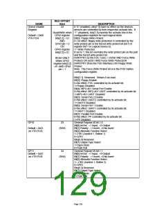
REG OFFSET
NAME
SMI_STS2
(hex)
11
DESCRIPTION
SMI Status Register 2
This register is used to read the status of the SMI inputs.
Default = 0x00
on VTR POR
(R/W)
Bit[0] MINT. Cleared at source.
Bit[1] KINT. Cleared at source.
Bit[2] IRINT. This bit is set by a transition on the IR pin
(IRRX or IRRX2 as selected in CR L5-F1-B6 i.e., after the
MUX). Cleared by a read of this register.
Bit[3] Reserved
Bit[4] P12. Cleared at source.
Bit[7:5] Reserved
SMI_STS3
12
SMI Status Register 3
This register is used to read the status of the SMI inputs.
Default = 0x00
on VTR POR
(R/W)
The following bits are cleared on a write of ‘1’.
Bit[0] GP20
Bit[1] GP21
Bit[2] GP22
Bit[3] Reserved
Bit[4] GP24
Bit[5] GP25
Bit[6] GP26
Bit[7] GP60
SMI_STS4
13
SMI Status Register 4
This register is used to read the status of the SMI inputs.
Default = 0x00
on VTR POR
(Note 6)
(R/W)
The following bits are cleared on a write of ‘1’.
Bit[0] GP30
Bit[1] GP31
Bit[2] GP32
Bit[3] GP33
Bit[4] GP41
Bit[5] GP42
Bit[6] GP43
Bit[7] GP61
SMI_STS5
14
SMI Status Register 5
This register is used to read the status of the SMI inputs.
The following bits are cleared on a write of ‘1’.
Bit[0] GP54
Default = 0x00
on VTR POR
(R/W)
Bit[1] GP55
Bit[2] GP56
Bit[3] GP57
Bit[4] Reserved
Bit[5] Reserved
Bit[6] FAN_TACH1
Bit[7] FAN_TACH2
Reserved – reads return 0
N/A
15
(R)
Page 125

 SMSC [ SMSC CORPORATION ]