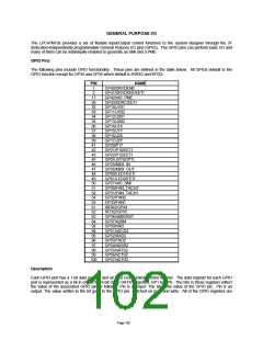
GENERAL PURPOSE I/O
The LPC47M10x provides a set of flexible Input/Output control functions to the system designer through the 37
dedicated independently programmable General Purpose I/O pins (GPIO). The GPIO pins can perform basic I/O and
many of them can be individually enabled to generate an SMI and a PME.
GPIO Pins
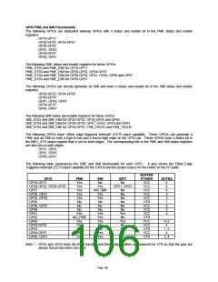
The following pins include GPIO functionality. These pins are defined in the table below. All GPIOs default to the
GPIO function except for GP34 and GP35 which default to IRRX2 and IRTX2.
PIN
1
NAME
GP40/DRVDEN0
2
GP41/DRVDEN1/EETI
GP42/nIO_PME
GP43/DDRC/EETI
GP10/J1B1
GP11/J1B2
GP12/J2B1
GP13/J2B2
GP14/J1X
GP15/J1Y
GP16/J2X
17
28
32
33
34
35
36
37
38
39
41
42
43
45
46
47
48
49
50
51
52
54
55
61
62
63
64
92
94
95
96
97
98
99
100
GP17/J2Y
GP20/P17
GP21/P16/EETI
GP22/P12/EETI
GP24 (SYSOPT)
GP25/MIDI_IN
GP26/MIDI_OUT
GP60/LED1/EETI
GP61/LED2/EETI
GP27/nIO_SMI
GP30/FAN_TACH2
GP31/FAN_TACH1
GP32/FAN2
GP33/FAN1
IRRX2/GP34
IRTX2/GP35
GP36/nKBDRST
GP37/A20M
GP50/nRI2
GP51/nDCD2
GP52/RXD2
GP53/TXD2
GP54/nDSR2
GP55/nRTS2
GP56/nCTS2
GP57/nDTR2
Description
Each GPIO port has a 1-bit data register and an 8-bit configuration control register. The data register for each GPIO
port is represented as a bit in one of the 8-bit GPIO DATA Registers, GP1 to GP6. The bits in these registers reflect
the value of the associated GPIO pin as follows. Pin is an input: The bit is the value of the GPIO pin. Pin is an
output: The value written to the bit goes to the GPIO pin. Latched on read and write. All of the GPIO registers are
Page 102

 SMSC [ SMSC CORPORATION ]