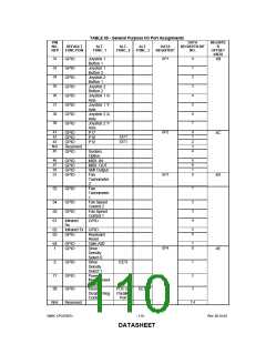
Note 6: These pins cannot be used for wakeup events to generate a PME while the part is under VTR
power (VCC=0). The GP32, GP33 and GP53 pins come up as output and low on a VCC POR
and hard reset.
Note 7: GP43 defaults to the GPIO function on VCC POR and Hard Reset.
Note 8: Since GP27 can be used to generate an SMI and as the nIO_SMI output, do not enable GP27
to generate an SMI (by setting bit 7 of the SMI Enable Register 3) if the nIO_SMI function is
selected on the GP27 pin. Use GP27 to generate an SMI event only if the SMI output is
enabled on the Serial IRQ stream.
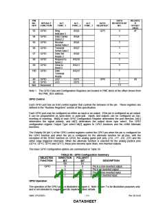
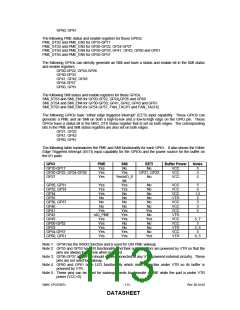
EITHER EDGE TRIGGERED INTERRUPTS
Six GPIO pins are implemented such that they allow an interrupt (PME or SMI) to be generated on both
a high-to-low and a low-to-high edge transition, instead of one or the other as selected by the polarity
bit.
The either edge triggered interrupts (EETI) function as follows: If the EETI function is selected for the
GPIO pin, then the bits that control input/output, polarity and open drain/push-pull have no effect on the
function of the pin. However, the polarity bit does affect the value of the GP bit (i.e., register GP2, bit 2
for GP22).
A PME or SMI interrupt occurs if the PME or SMI enable bit is set for the corresponding GPIO and the
EETI function is selected on the GPIO. The PME or SMI status bits are set when the EETI pin
transitions (on either edge) and are cleared on a write of ‘1’. There are also status bits for the EETIs
located in the MSC_STS register, which are also cleared on a write of ‘1’. The MSC_STS register
provides the status of all of the EETI interrupts within one register. The PME, SMI or MSC status is
valid whether or not the interrupt is enabled and whether or not the EETI function is selected for the pin.
Miscellaneous Status Register (MSC_STS) is for the either edge triggered interrupt status bits. If the
EETI function is selected for a GPIO then both a high-to-low and a low-to-high edge will set the
corresponding MSC status bits. Status bits are cleared on a write of ‘1’. See Runtime Register section
for more information.
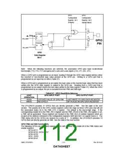
LED FUNCTIONALITY
The LPC47B27x provides LED functionality on two GPIOs, GP60 and GP61. These pins can be
configured to turn the LED on and off and blink independent of each other through the LED1 and LED2
runtime registers at offset 0x5D and 0x5E from the base address located in the primary base I/O
address in Logical Device A.
The LED pins (GP60 and GP61) are able to control the LED while the part is under VTR power with
VCC removed. In order to control a LED while the part is under VTR power, the GPIO pin must be
configured for the LED function and either open drain or push-pull buffer type. In the case of open-drain
buffer type, the pin is capable of sinking current to control the LED. In the case of push-pull buffer type,
the part will source current. The part is also able to blink the LED under VTR power. The LED will not
blink under VTR power (VCC removed) if the external 32kHz clock is not connected.
The LED pins can drive a LED when the buffer type is configured to be push-pull and the part is
powered by either VCC or VTR, since the buffers for these pins are powered by VTR. This means they
will source their specified current from VTR even when VCC is present.
The LED control registers are defined in the “Runtime Register” section.
WATCH DOG TIMER
The LPC47B27x contains a Watch Dog Timer (WDT). The Watch Dog Time-out status bit may be mapped
to an interrupt through the WDT_CFG Runtime Register.
The LPC47B27x's WDT has a programmable time-out ranging from 1 to 255 minutes with one minute
resolution, or 1 to 255 seconds with 1 second resolution. The units of the WDT timeout value are selected
via bit[7] of the WDT_TIMEOUT register (Runtime Register at offset 0x52). The WDT time-out value is set
through the WDT_VAL Runtime register. Setting the WDT_VAL register to 0x00 disables the WDT
function (this is its power on default). Setting the WDT_VAL to any other non-zero value will cause the
WDT to reload and begin counting down from the value loaded. When the WDT count value reaches zero
SMSC LPC47B27x
- 114 -
Rev. 08-10-04
DATASHEET

 SMSC [ SMSC CORPORATION ]