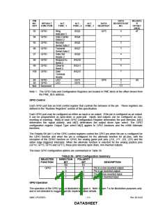
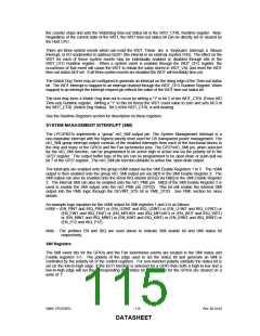
PIN
NO.
DATA
REGISTER BIT
NO.
REGISTE
R
DEFAULT
ALT.
ALT.
ALT.
DATA
/QFP
FUNCTION
FUNC. 1
FUNC. 2
FUNC. 3
REGISTER1
OFFSET
(HEX)
4F
0
1
2
3
4
5
6
7
92
94
95
96
97
98
99
100
GPIO
GPIO
GPIO
GPIO
GPIO
GPIO
GPIO
GPIO
Ring
IRQ3
IRQ4
GP5
Indicator 2
Data Carrier
Detect 2
Receive
Serial Data 2
Transmit
Serial Data 2
Data Set
Ready 2
Request to
Send 2
IRQ5
IRQ7
IRQ9
IRQ10
IRQ11
IRQ15
Clear to
Send 2
Date
Terminal
Ready
0
1
7:2
48
49
N/A
GPIO
LED
EETI
EETI
GP6
50
GPIO
LED
Reserved
Note 1: The GPIO Data and Configuration Registers are located in PME block at the offset shown from
the PME_BLK address.
GPIO Control
Each GPIO port has an 8-bit control register that controls the behavior of the pin. These registers are
defined in the “Runtime Registers” section of this specification.
Each GPIO port may be configured as either an input or an output. If the pin is configured as an output,
it can be programmed as open-drain or push-pull. Inputs and outputs can be configured as non-
inverting or inverting. Bit[0] of each GPIO Configuration Register determines the port direction, bit[1]
determines the signal polarity, and bit[7] determines the output driver type select. The GPIO
configuration register Output Type select bit[7] applies to GPIO functions and the nSMI Alternate
functions.
The Polarity Bit (bit 1) of the GPIO control registers control the GPIO pin when the pin is configured for
the GPIO function and when the pin is configured for the alternate function for all pins, with the
exception of the DDRC function on GP43, the analog game port pins (J1X, J1Y, J2X, J2Y) and the
either edge triggered interrupts. When the alternate function is selected for the analog joystick pins
(GP14, GP15, GP16 and GP17), these pins become open drain, non-inverted outputs.
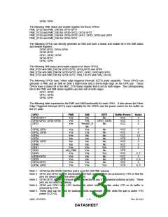
The basic GPIO configuration options are summarized in Table 56.
TABLE 56 - GPIO Configuration Summary
SELECTED
FUNCTION
DIRECTION
POLARITY
BIT
B0
0
BIT
B1
0
DESCRIPTION
GPIO
Pin is a non-inverted output.
Pin is an inverted output.
Pin is a non-inverted input.
Pin is an inverted input.
0
1
1
0
1
1
GPIO Operation
The operation of the GPIO ports is illustrated in Figure 4. Note: Figure 7 is for illustration purposes only
and is not intended to suggest specific implementation details.
SMSC LPC47B27x
- 111 -
Rev. 08-10-04
DATASHEET

 SMSC [ SMSC CORPORATION ]