0=The group SMI output is inactive.
1=The group SMI output is active.
Note: Bit 5 of the SMI_EN2 register must also be set.
This bit is cleared on a write of ‘1’.
There is a bit in the PME Enable Register 3 to enable the SMI onto the nIO_PME pin (if the nIO_PME
function is selected for GP42). This bit, DEVINT_EN, is at bit 3 of the PME_EN3 register. This bit will
enable the internal “group” SMI signal (if bit 5 of the SMI_EN2 register is set) into the PME logic through
the DEVINT_STS bit as follows: If the DEVINT_EN bit is ‘1’ and the DEVINT_STS bit is ‘1’ then the
nIO_PME pin will be active. This pin has its polarity controlled by the polarity bit in the GP42 register.
This bit is defined as follows:
0=Disable group SMI output from the nIO_PME pin.
1=Enable group SMI output onto the nIO_PME pin. That is, if this bit is set and the DEVINT_STS bit is
set then a nPME is generated.
Note: Bit 5 of the SMI_EN2 register must also be set.
‘WAKE ON SPECIFIC KEY’ OPTION
The LPC47B27x has logic to detect a single keyboard scan code for wakeup (PME generation). The
scan code is programmed onto the Keyboard Scan Code Register, a runtime register at offset 0x5F
from the base address located in the primary base I/O address in Logical Device A. This register is
powered by VTR and reset on VTR POR.
The PME status bit for this event is located in the PME_STS1 register at bit 5 and the PME enable bit
for this event is located in the PME_EN1 register at bit 5. See the Runtime Register section for a
definition of these registers.
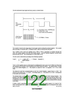
Data transmissions from the keyboard consist of an 11-bit serial data stream. A logic 1 is sent at an
active high level. The following table shows the functions of the bits.
BIT
1
FUNCTION
Start bit (always 0)
2
Data bit 0 (least significant bit)
Data bit 1
3
4
Data bit 2
5
Data bit 3
6
Data bit 4
7
Data bit 5
8
Data bit 6
9
Data bit 7 (most significant bit)
Parity bit (odd parity)
Stop Bit (always 1)
10
11
The timing for the keyboard clock and data signals are shown in the “Timing Diagrams” section.
The CLK32_PRSN bit (bit 0 of the CLOCKI32 register at 0xF0 in Logical Device A) will determine the
clock source for this feature when the part is powered by VCC. If the external 32kHz clock is not
connected, the 32kHz internal signal is derived from the 14MHz clock when VCC is active. Use the
32kHz clock for this feature when the part is under trickle power. This feature will not work when the
part is under trickle power (VCC removed) if the external 32kHz clock is not connected.
The SPEKEY_EN bit at bit 1 of the CLOCKI32 register at 0xF0 in Logical Device A is used to control
this feature. This bit is used to turn the logic for this feature on and off. It will disable the 32kHz clock
input to the logic. The logic will draw no power when disabled. The bit is defined as follows:
0= “Wake on specific key” logic is on (default)
1= “Wake on specific key” logic is off
SMSC LPC47B27x
- 118 -
Rev. 08-10-04
DATASHEET

 SMSC [ SMSC CORPORATION ]