High Performance Two Port 10/100 Managed Ethernet Switch with 32-Bit Non-PCI CPU Interface
Datasheet
8.4
Host Interface Timing
This section details the characteristics and special restrictions of the various supported host cycles.
For detailed timing specifications on supported PIO read/write operations, refer to Section 15.5, "AC
Specifications". The LAN9312 supports the following host cycles:
Read Cycles:
PIO Reads (nCS or nRD controlled)
PIO Burst Reads (nCS or nRD controlled)
RX Data FIFO Direct PIO Reads (nCS or nRD controlled)
RX Data FIFO Direct PIO Burst Reads (nCS or nRD controlled)
Write Cycles:
PIO Writes (nCS or nWR controlled)
TX Data FIFO Direct PIO Writes (nCS or nWR controlled)
8.4.1
Special Situations
8.4.1.1
Reset Ending During a Read Cycle
If a reset condition terminates during an active read cycle, the tail end of the read cycle will be ignored
by the LAN9312.
8.4.1.2
Writes Following a Reset
Following any reset, writes from the host bus are ignored until after a read cycle is performed.
8.4.2
Special Restrictions on Back-to Back Write-Read Cycles
It is important to note that there are specific restrictions on the timing of back-to-back host write-read
operations. These restrictions concern reading the host control registers after any write cycle to the
LAN9312. In some cases there is a delay between writing to the LAN9312, and the subsequent side
effect (change in the control register value). For example, when writing to the TX Data FIFO, it takes
up to 135ns for the level indication to change in the TX FIFO Information Register (TX_FIFO_INF).
In order to prevent the host from reading stale data after a write operation, minimum wait periods have
been established. These periods are specified in Table 8.1. The host processor is required to wait the
specified period of time after any write to the LAN9312 before reading the resource specified in the
table. These wait periods are for read operations that immediately follow any write cycle. Note that the
required wait period is dependant upon the register being read after the write.
Performing “dummy” reads of the Byte Order Test Register (BYTE_TEST) register is a convenient way
to guarantee that the minimum write-to-read timing restriction is met. Table 8.1 shows the number of
dummy reads that are required before reading the register indicated. The number of BYTE_TEST
reads in this table is based on the minimum timing for Tcyc (45ns). For microprocessors with slower
busses the number of reads may be reduced as long as the total time is equal to, or greater than the
time specified in the table. Note that dummy reads of the BYTE_TEST register are not required as
long as the minimum time period is met.
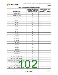
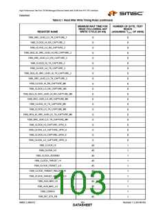
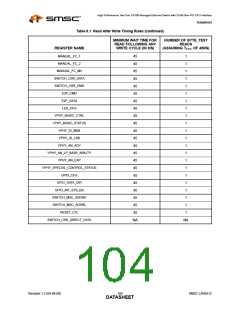
Table 8.1 Read After Write Timing Rules
MINIMUM WAIT TIME FOR
READ FOLLOWING ANY
WRITE CYCLE (IN NS)
NUMBER OF BYTE_TEST
READS
(ASSUMING TCYC OF 45NS)
REGISTER NAME
RX Data FIFO
0
0
SMSC LAN9312
101
Revision 1.2 (04-08-08)
DATASHEET

 SMSC [ SMSC CORPORATION ]