Non-PCI Single-Chip Full Duplex Ethernet Controller with Magic Packet
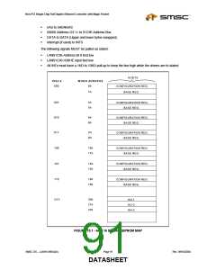
On EEPROM write operations (after setting the STORE bit) the value of the GENERAL PURPOSE
REGISTER is written at the EEPROM word address defined by the POINTER REGISTER 6 least
significant bits.
RELOAD and STORE are set by the user to initiate read and write operations respectively. Polling the
value until read low is used to determine completion. When an EEPROM access is in progress the
STORE and RELOAD bits of CTR will read-back as both bits high. No other bits of the LAN91C96
can be read or written until the EEPROM operation completes and both bits are clear. This
mechanism is also valid for reset initiated reloads.
Note:
If no EEPROM is connected to the LAN91C96, the ENEEP pin should be grounded and no accesses to
the EEPROM will be attempted. Configuration, Base and Individual Addresses assume their default values
upon hardware reset and the CPU is responsible for programming them for their final value.
10.1 Diagnostic LEDs
The following LED drive signals are available for diagnostic and installation aid purposes:
nTXLED - Activated by transmit activity.
nBSELED - Board select LED. Activated when the board space is accessed, namely on accesses to the
LAN91C96 register space or the ROM area decoded by the LAN91C96. The signal is stretched to 125
msec.
nRXLED - Activated by receive activity.
nLINKLED - Reflects the link integrity status.
10.2 Bus Clock Considerations
The arbiter exploits the sequential nature of the CPU accesses to provide a very fast access time.
Memory bandwidth considerations will have an effect on the CPU cycle time but no effect on access time.
For normal 8MHz, 10MHz, and 12.5MHz LOCAL BUS, as well as EISA normal cycles, the LAN91C96 can
be accessed without negating ready.
See Arbitration Considerations in Functional Description of the Blocks for more details.
10.3 68000 Bus Interface
The LAN91C96 enters the 68000 interface mode when nIORD and nIOWR are asserted simultaneously.
Once the two are asserted together, the only way to return to the LOCAL BUS interface is by hard
resetting the chip. Notice that the chip is required to power up in LOCAL BUS mode to use the 68000
interface.
For the first chip access, the first transfer (to the LAN91C96) must be a write. The LAN91C96 uses this
write to confirm the 68000 mode. An attempted read may return incorrect data. The LAN91C96 responds
to addresses per the base address register contents (as in LOCAL BUS mode). Notice that the worst case
access time for the first cycle is the same as that for LOCAL BUS or PCMCIA modes.
The following is the Motorola 68000 Processor and the LAN91C96 pin mapping:
DS, LDS, or UDS to nIORD/xDS
R/nW to nIOWR/R/nW
Rev. 09/10/2004
Page 90
SMSC LAN91C965v&3v
DATASHEET

 SMSC [ SMSC CORPORATION ]