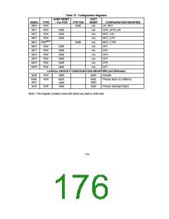
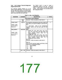
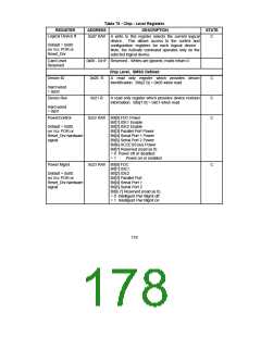
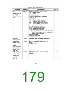
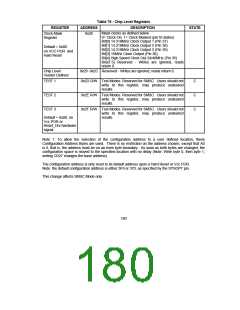
Table 76 - Chip Level Registers
DESCRIPTION
REGISTER
Clock Mask
ADDRESS
STATE
Mask clocks as defined below.
0x28
0= Clock On, 1= Clock Masked (pin tri-states)
Bit[0] 14.318MHz Clock Output 1 (Pin 37)
Bit[1] 14.318MHz Clock Output 2 (Pin 38)
Bit[2] 14.318MHz Clock Output 3 (Pin 39)
Bit[3] 16MHz Clock Output (Pin 36)
Bit[4] High Speed Clock Out 24/48MHz (Pin 35)
Bits[7:5] Reserved - Writes are ignored, reads
return 0.
Register
Default = 0x00
on VCC POR and
Hard Reset
Chip Level
0x29 -0x2C Reserved - Writes are ignored, reads return 0.
Vendor Defined
TEST 1
TEST 2
TEST 3
0x2D R/W Test Modes: Reserved for SMSC. Users should not
write to this register, may produce undesired
results.
C
C
C
0x2E R/W Test Modes: Reserved for SMSC. Users should not
write to this register, may produce undesired
results.
0x2F R/W Test Modes: Reserved for SMSC. Users should not
write to this register, may produce undesired
results.
Default = 0x00, on
Vcc POR or
Reset_Drv hardware
signal.
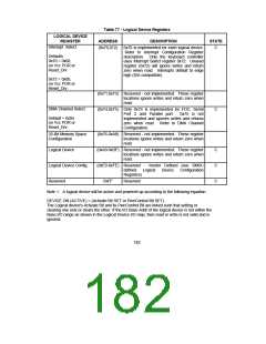
Note 1: To allow the selection of the configuration address to a user defined location, these
Configuration Address Bytes are used. There is no restriction on the address chosen, except that A0
is 0, that is, the address must be on an even byte boundary. As soon as both bytes are changed, the
configuration space is moved to the specified location with no delay (Note: Write byte 0, then byte 1;
writing CR27 changes the base address).
The configuration address is only reset to its default address upon a Hard Reset or Vcc POR.
Note: the default configuration address is either 3F0 or 370, as specified by the SYSOPT pin.
This change affects SMSC Mode only.
180

 SMSC [ SMSC CORPORATION ]