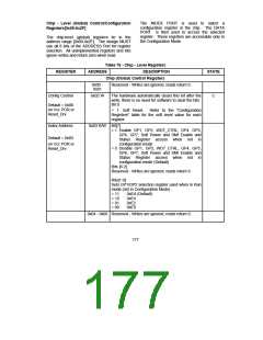
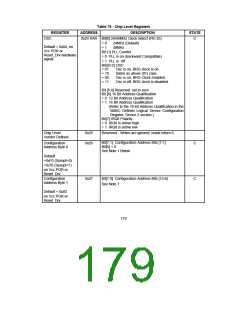
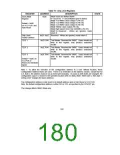
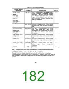
Table 76 - Chip - Level Registers
REGISTER
ADDRESS
DESCRIPTION
STATE
Logical Device #
0x07 R/W A write to this register selects the current logical
device. This allows access to the control and
configuration registers for each logical device.
Note: the Activate command operates only on the
selected logical device.
C
Default = 0x00
on Vcc POR or
Reset_Drv
Card Level
Reserved
0x08 - 0x1F
Reserved - Writes are ignored, reads return 0.
Chip Level, SMSC Defined
Device ID
0x20 R
A
read only register which provides device
C
C
C
identification. Bits[7:0] = 0x03 when read
Hard wired
= 0x03
Device Rev
0x21 R
A read only register which provides device revision
information. Bits[7:0] = 0x01 when read
Hard wired
= 0x01
PowerControl
0x22 R/W Bit[0] FDC Power
Bit[1] IDE1 Enable
Default = 0x00.
on Vcc POR or
Reset_Drv hardware
signal.
Bit[2] IDE2 Enable
Bit[3] Parallel Port Power
Bit[4] Serial Port 1 Power
Bit[5] Serial Port 2 Power
Bit[6] ACCESS.bus Power
Bit[7] Reserved (read as 0)
= 0 Power off or disabled
= 1
Power on or enabled
Power Mgmt
0x23 R/W Bit[0] FDC
Bit[1] IDE1
C
Default = 0x00.
on Vcc POR or
Reset_Drv hardware
signal
Bit[2] IDE2
Bit[3] Parallel Port
Bit[4] Serial Port 1
Bit[5] Serial Port 2
Bit[6:7] Reserved (read as 0)
= 0 Intelligent Pwr Mgmt off
= 1 Intelligent Pwr Mgmt on
178

 SMSC [ SMSC CORPORATION ]