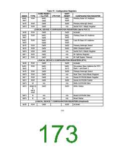
CONFIGURATION
The Configuration of the FDC37C93xFR is very
configuration ports to initialize the logical
devices at POST. The INDEX and DATA ports
are only valid when the FDC37C93xFR is in
Configuration Mode.
flexible and is based on the configuration
architecture implemented in typical Plug-and-
Play components. The FDC37C93xFR is
designed for motherboard applications in which
the resources required by their components are
known. With its flexible resource allocation
architecture, the FDC37C93xFR allows the
BIOS to assign resources at POST.
The SYSOPT pin is latched on the falling edge
of the RESET_DRV or on Vcc Power On Reset
to determine the configuration register's base
address. The SYSOPT pin is used to select the
CONFIG PORT's I/O address at power-up.
Once powered up the configuration port base
address can be changed through configuration
registers CR26 and CR27. The SYSOPT pin
is a hardware configuration pin which is
shared with the nRTS1 signal on pin 148.
During reset this pin is a weak active low signal
which sinks 30µA. Note: All I/O addresses are
qualified with AEN.
SYSTEM ELEMENTS
Primary Configuration Address Decoder
After a hard reset (RESET_DRV pin asserted) or
Vcc Power On Reset the FDC37C93xFR is in
the Run Mode with all logical devices disabled.
The logical devices may be configured through
two standard Configuration I/O Ports (INDEX
and DATA) by placing the FDC37C93xFR into
Configuration Mode. The BIOS uses these
The INDEX and DATA ports are effective only
when the chip is in the Configuration State.
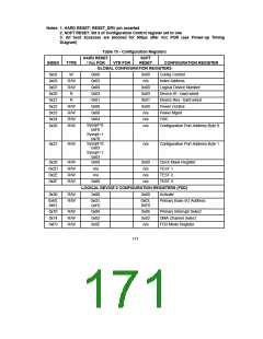
SYSOPT= 0
(Pull-down resistor)
SYSOPT= 1
PORT NAME
CONFIG PORT (Note 2)
INDEX PORT (Note 2)
DATA PORT
Refer to Note 1
(10K Pull-up resistor)
TYPE
0x03F0
0x0370
Write
0x03F0
0x0370
Write
INDEX PORT + 1
Read/Write
Note 1: If using TTL RS232 drivers use 1K pull-down. If using CMOS RS232 drivers use
10K pull-down.
Note 2: The configuration port base address can be relocated through CR26 and CR27.
Entering the Configuration State
Exiting the Configuration State
The device enters the Configuration State when
the following Config Key is successfully written
to the CONFIG PORT.
The device exits the Configuration State when
the following Config Key is successfully written
to the CONFIG PORT.
Config Key = < 0x55, 0x55>
Config Key = < 0xAA>
169

 SMSC [ SMSC CORPORATION ]