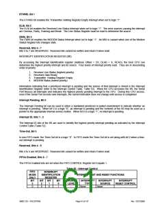
MODEM CONTROL REGISTER (MCR)
The Modem Control register (Address Offset = 4H, DLAB = X, READ/WRITE) manages the interface for the MODEM,
data set, or device emulating a MODEM.
Data Terminal Ready, Bit 0
The Data Terminal Ready bit controls the Data Terminal Ready (nDTR) output. When bit 0 is set to a logic “1”,
the nDTR output is forced to a logic “0”. When bit 0 is a logic “0”, the nDTR output is forced to a logic “1”.
Request To Send, Bit 1
The Request To Send bit controls the Request To Send (nRTS) output. . When bit 1 is set to a logic “1”, the
nRTS output is forced to a logic “0”. When bit 1 is a logic “0”, the nRTS output is forced to a logic “1”.
OUT1, Bit 2
The OUT1 bit controls the Output 1 (OUT1) bit. This bit does not have an output pin and can only be read or written
by the CPU.
OUT2, Bit 3
The OUT2 bit is used to enable the UART interrupt. When OUT2 is a logic “0”, the serial port interrupt output is
forced to a high impedance state; i.e, disabled. When OUT2 is a logic “1”, the serial port interrupt outputs are
enabled.
Loop, Bit 4
The Loop bit provides the loopback feature for diagnostic testing of the Serial Port. When bit 4 is set to logic “1”, the
following occurs:
1. The TXD is set to the Marking State (logic “1”).
2. The receiver Serial Input (RXD) is disconnected.
3. The output of the Transmitter Shift Register is “looped back” into the Receiver Shift Register input.
4. All MODEM Control inputs (nCTS, nDSR, nRI and nDCD) are disconnected.
5. The four MODEM Control outputs (nDTR, nRTS, OUT1 and OUT2) are internally connected to the four
MODEM Control inputs (nDSR, nCTS, RI and DCD) respectively.
6. The Modem Control output pins are forced inactive.
7. Data that is transmitted is immediately received.
The Loopback feature allows the processor to verify the transmit and receive data paths of the Serial Port. The
receiver and the transmitter interrupts are fully operational in loopback mode. The MODEM Control Interrupts are
also operational but the interrupts’ sources are now the lower four bits of the MODEM Control Register instead of the
MODEM Control inputs. The interrupts are still controlled by the Interrupt Enable Register.
Reserved, Bits 5 - 7
Bits 5 to 7 are RESERVED. Reserved bits cannot be written and return 0 when read.
LINE STATUS REGISTER (LSR)
Address Offset = 5H, DLAB = X, READ/WRITE
Data Ready, Bit 0
Data Ready (DR) is set to a logic “1” whenever a complete received data character has been transferred into the
Receiver Buffer Register or the FIFO. DR is reset to a logic “0” by reading all of the data in the Receive Buffer
Register or the FIFO.
SMSC DS – FDC37N769
Page 65 of 137
Rev. 12/21/2000

 SMSC [ SMSC CORPORATION ]