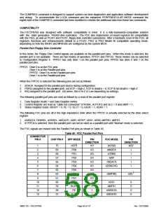
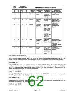
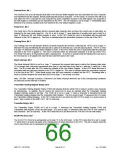
FIFO
MODE
ONLY
BIT
INTERRUPT
IDENTIFICATION
REGISTER
INTERRUPT SET AND RESET FUNCTIONS
BIT
2
BIT
1
BIT
0
PRIORITY
LEVEL
INTERRUPT
TYPE
INTERRUPT
SOURCE
INTERRUPT
3
RESET CONTROL
0
1
1
0
Highest
Receiver Line Overrun Error, Reading the Line
Status
Parity Error,
Framing Error
or Break
Status Register
Interrupt
0
1
1
1
0
0
0
0
Second
Second
Received
Data
Receiver Data Read Receiver
Available
Buffer or the FIFO
drops below the
trigger level.
Available
Character
Time-out
Indication
No Characters Reading the
Have Been
Removed
Receiver Buffer
Register
From or Input
to the RCVR
FIFO during
the last 4
Character
times and there
is at least 1
character in it
during this time
Transmitter
Holding
0
0
0
0
1
0
0
0
Third
Transmitter
Holding
Reading the IIR
Register (if Source
Register
Empty
Register Empty of Interrupt) or
Writing the
Transmitter Holding
Register
Fourth
MODEM
Status
Clear to Send
or Data Set
Reading the
MODEM Status
Ready or Ring Register
Indicator or
Data Carrier
Detect
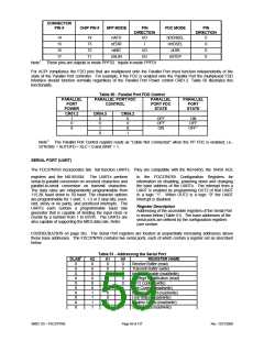
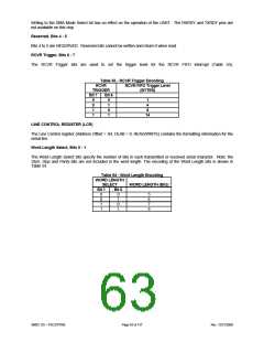
FIFO CONTROL REGISTER (FCR)
The FIFO Control register (Address Offset = 2H, DLAB = X, WRITE) appears at the same location as the IIR. This
register is used to enable and clear the FIFOs and set the RCVR FIFO trigger level. Note: DMA is not supported.
FIFO Enable, Bit 0
Setting the FIFO Enable bit to a logic “1” enables both the XMIT and RCVR FIFOs. Clearing this bit to a logic “0”
disables both the XMIT and RCVR FIFOs and clears all bytes from both FIFOs. When changing from FIFO Mode to
non-FIFO (16450) mode, data is automatically cleared from the FIFOs. This bit must be a 1 when other bits in this
register are written to or they will not be properly programmed.
RCVR FIFO Reset, Bit 1
Setting the RCVR FIFO Reset bit to a logic “1” clears all bytes in the RCVR FIFO and resets its counter logic to 0.
The shift register is not cleared. This bit is self-clearing.
XMIT FIFO Reset, Bit 2
Setting the XMIT FIFO Reset bit to a logic “1” clears all bytes in the XMIT FIFO and resets its counter logic to 0. The
shift register is not cleared. This bit is self-clearing.
DMA Mode Select, Bit 3
SMSC DS – FDC37N769
Page 62 of 137
Rev. 12/21/2000

 SMSC [ SMSC CORPORATION ]