SIRQ_EN
nCLKRUN
DRIVEN BY 869
869 STOPS DRIVING
nCLKRUN
ANY IRQ CHANGE1,2
nCLKRUN
CLK33
2 CLKS
MIN.
FIGURE 7 - CLOCK START ILLUSTRATION
Note 1:
Note 2:
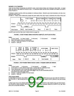
The signal “ANY IRQ CHANGE” is the same as “CHANGE” in Table 72.
The FDC37N3869 must continually monitor the state of nCLKRUN to maintain the PCI Clock
until an active “ANY IRQ CHANGE” condition has been transferred to the host in a Serial IRQ
cycle. For example, if “ANY IRQ CHANGE” is asserted before nCLKRUN is de-asserted (not
shown in Figure 7), the FDC37N3869 must assert nCLKRUN as needed until the Serial IRQ
cycle has completed.
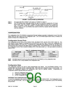
CONFIGURATION
The configuration of the FDC37N3869 is programmed through hardware selectable Configuration Access Ports that
appear when the chip is placed into the configuration state. The FDC37N3869 logical device blocks, if enabled, will
operate normally in the configuration state.
Configuration Access Ports
The Configuration Access Ports are the CONFIG PORT, the INDEX PORT, and the DATA PORT (Table 75). The
base address of these registers is controlled by the nRTS2/SYSOPT pin (see Table 1) and by the Configuration Port
Base Address registers CR12 and CR13. To determine the configuration base address at power-up, the state of the
nRTS2/SYSOPT pin is latched by the falling edge of a hardware reset. If the latched state is a 0, the base address of
the Configuration Access Ports is located at address 3F0H; if the latched state is a 1, the base address is located at
address 370H.
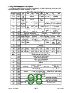
Table 75 - Configuration Access Ports
PORT NAME
CONFIG PORT
INDEX PORT
DATA PORT
SYSOPT = 0
0x3F0
SYSOPT = 1
0x370
TYPE
WRITE
0x3F0
0x370
READ/WRITE1,2
READ/WRITE1
INDEX PORT + 1
Note1: The INDEX and DATA ports are active only when the FDC37N3869 is in the configuration state.
Note2: The INDEX PORT is only readable in the configuration state.
Configuration State
The configuration registers are used to select programmable chip options. The FDC37N3869 operates in two
possible states: the run state and the configuration state. After power up by default the chip is in the run state. To
program the configuration registers, the configuration state must be explicitly enabled. Programming the
configuration registers typically follows this sequence:
1)
2)
3)
Enter the Configuration State,
Program the Configuration Register(s),
Exit the Configuration State.
ENTERING THE CONFIGURATION STATE
To enter the configuration state write the Configuration Access Key to the CONFIG PORT. The Configuration Access
Key is one byte of 55H data. The FDC37N3869 will automatically activate the Configuration Access Ports following
this procedure.
SMSC DS – FDC37N3869
Page 96
Rev. 10/25/2000

 SMSC [ SMSC CORPORATION ]