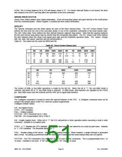
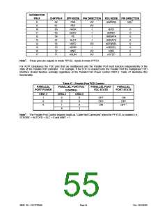
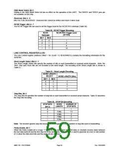
CONNECTOR
PIN #
8
9
CHIP PIN #
SPP MODE PIN DIRECTION
FDC MODE PIN DIRECTION
(nMTR0)
62
61
60
59
58
57
74
73
72
71
PD6
PD7
nACK
BUSY
PE
I/O
I/O
I
I
I
I/(0) 1
10
11
12
13
14
15
16
17
nDS1
nMTR1
0
0
0
0
0
0
0
0
nWDATA
nWGATE
nDENSEL
nHDSEL
nDIR
SLCT
nAFD
nERR
nINIT
nSLIN
I
I/O
I
I/O
I/O
nSTEP
Note1: These pins are outputs in mode PPFD2. Inputs in mode PPFD1
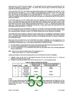
For ACPI compliance the FDD pins that are multiplexed onto the Parallel Port must function independently of the
state of the Parallel Port controller. For example, if the FDC is enabled onto the Parallel Port the multiplexed FDD
Interface should function normally regardless of the Parallel Port Power control CR01.2. Table 47 illustrates this
functionality.
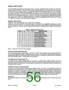
Table 47 - Parallel Port FDD Control
PARALLEL
PARALLEL PORT FDC
CONTROL
PARALLEL PORT
PARALLEL
PORT POWER
FDC STATE
PORT STATE
CR01.2
CR04.3
CR04.2
1
0
X
0
0
1
X
0
0
X
1
OFF
OFF
ON
ON
OFF
OFF1
Note1: The Parallel Port Control register reads as “Cable Not Connected” when the PP FDC is enabled; i.e.,
STROBE = AUTOFD = SLC = 0 and nINIT = 1
SMSC DS – FDC37N3869
Page 55
Rev. 10/25/2000

 SMSC [ SMSC CORPORATION ]