SERIAL PORT (UART)
The FDC37N3869 incorporates two full function UARTs. They are compatible with the NS16450, the 16450 ACE
registers and the NS16550A. The UARTs perform serial-to-parallel conversion on received characters and parallel-
to-serial conversion on transmit characters. The data rates are independently programmable from 115.2K baud down
to 50 baud. The character options are programmable for 1 start; 1, 1.5 or 2 stop bits; even, odd, sticky or no parity;
and prioritized interrupts. The UARTs each contain a programmable baud rate generator that is capable of dividing
the input clock or crystal by a number from 1 to 65535. The UARTs are also capable of supporting the MIDI data
rate. Refer to the FDC37N3869 Configuration Registers for information on disabling, powering down and changing the
base address of the UARTs. The interrupt from a UART is enabled by programming OUT2 of that UART to a logic
“1”. When OUT2 is a logic “0” the UART Interrupt is disabled.
Register Description
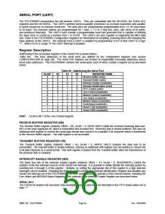
Addressing of the accessible registers of the Serial Port is shown below (
Table 48). The base addresses of the serial ports are defined by the configuration registers (see section
CONFIGURATION on page 96). The Serial Port registers are located at sequentially increasing addresses above
these base addresses. The FDC37N3869 contains two serial ports, each of which contain a register set as described
below.
Table 48 - Addressing the Serial Port
DLAB1
A2
0
0
0
0
0
0
1
1
1
1
0
0
A1
0
0
0
1
1
1
0
0
1
1
0
0
A0
0
0
1
0
0
1
0
1
0
1
0
1
REGISTER NAME
0
0
Receive Buffer (read)
Transmit Buffer (write)
0
Interrupt Enable (read/write)
Interrupt Identification (read)
FIFO Control (write)
Line Control (read/write)
Modem Control (read/write)
Line Status (read/write)
Modem Status (read/write)
Scratchpad (read/write)
Divisor LSB (read/write)
Divisor MSB (read/write)
X
X
X
X
X
X
X
1
1
Note1: DLAB is Bit 7 of the Line Control Register
RECEIVE BUFFER REGISTER (RB)
The Receive Buffer register (Address Offset = 0H, DLAB = 0, READ ONLY) holds the received incoming data byte.
Bit 0 is the least significant bit, which is transmitted and received first. Received data is double buffered; this uses an
additional shift register to receive the serial data stream and convert it to a parallel 8 bit character which is transferred
to the Receive Buffer register. The shift register is not accessible.
TRANSMIT BUFFER REGISTER (TB)
The Transmit Buffer register (Address Offset = 0H, DLAB = 0, WRITE ONLY) contains the data byte to be
transmitted. The transmit buffer is double buffered, utilizing an additional shift register (not accessible) to convert the
8 bit data character to a serial format. This shift register is loaded from the Transmit Buffer when the transmission of
the previous byte is complete.
INTERRUPT ENABLE REGISTER (IER)
The lower four bits of the Interrupt Enable register (Address Offset = 1H, DLAB = 0, READ/WRITE) control the
enables of the five interrupt sources of the Serial Port interrupt. It is possible to totally disable the interrupt system by
resetting bits 0 through 3 of this register. Similarly, by setting the appropriate bits of this register to a high selected
interrupts can be enabled. Disabling the interrupt system inhibits the Interrupt Identification Register and disables any
Serial Port interrupt out of the FDC37N3869. All other system functions operate in their normal manner, including the
Line Status and MODEM Status Registers. The contents of the Interrupt Enable Register are described below.
ERDAI, Bit 0
The ERDAI bit enables the Received Data Available Interrupt (and time-out interrupts in the FIFO mode) when set to
logic “1”.
SMSC DS – FDC37N3869
Page 56
Rev. 10/25/2000

 SMSC [ SMSC CORPORATION ]