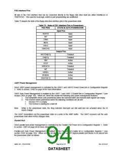
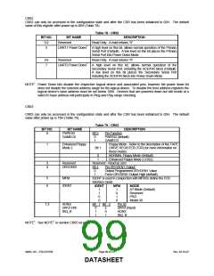
The EPP logic is in powerdown under any of the following conditions:
1. EPP is not enabled in the configuration registers.
2. EPP is not selected through ecr while in ECP mode.
The ECP logic is in powerdown under any of the following conditions:
1. ECP is not enabled in the configuration registers.
2. SPP, PS/2 Parallel port or EPP mode is selected through ecr while in ECP mode.
The parallel port logic can change powerdown modes when the ECP mode is changed through the ecr register or
when the parallel port mode is changed through the configuration registers.
CONFIGURATION
The configuration of the FDC37N769 is programmed through hardware selectable Configuration Access Ports that
appear when the chip is placed into the configuration state. The FDC37N769 logical device blocks, if enabled, will
operate normally in the configuration state.
Configuration Access Ports
The Configuration Access Ports are the CONFIG PORT, the INDEX PORT, and the DATA PORT (Table 74). The
base address of these registers is controlled by the nRTS2/SYSOPT pin (see Table 1). To determine the
configuration base address, the state of the nRTS2/SYSOPT pin is latched by the falling edge of a hardware reset. If
the latched state is a 0, the base address of the Configuration Access Ports is located at address 3F0H; if the latched
state is a 1, the base address is located at address 370H.
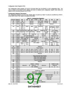
Table 74 - Configuration Access Ports
PORT NAME
CONFIG PORT
INDEX PORT
DATA PORT
SYSOPT = 0
0x3F0
SYSOPT = 1
0x370
TYPE
WRITE
0x3F0
0x370
READ/WRITE1,2
READ/WRITE1
INDEX PORT + 1
Note1: The INDEX and DATA ports are active only when the FDC37N769 is in the configuration state.
Note2: The INDEX PORT is only readable in the configuration state.
Configuration State
The configuration registers are used to select programmable chip options. The FDC37N769 operates in two possible
states: the run state and the configuration state. After power up by default the chip is in the run state. To program
the configuration registers, the configuration state must be explicitly enabled. Programming the configuration
registers typically follows this sequence:
1. Enter the Configuration State,
2. Program the Configuration Register(s),
3. Exit the Configuration State.
Entering the Configuration State
To enter the configuration state write the Configuration Access Key to the CONFIG PORT. The Configuration Access
Key is one byte of 55H data. The FDC37N769 will automatically activate the Configuration Access Ports following
this procedure.
Configuration Register Programming
The FDC37N769 contains configuration registers CR00-CR2F. After the FDC37N769 enters the configuration state,
configuration registers can be programmed by first writing the register index number (00 - 2FH) to the Configuration
Select Register (CSR) through the INDEX PORT and then writing or reading the configuration register contents
through the DATA PORT. Configuration register access remains enabled until the configuration state is explicitly
exited.
SMSC DS – FDC37N769
Page 95 of 137
Rev. 02-16-07
DATASHEET

 SMSC [ SMSC CORPORATION ]