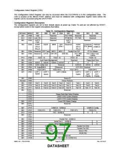
DEFAULT INDEX
DB7
DB6
Reserved
DB5
DB4
DB3
DB2
DB1
DB0
00H
03H
00H
00H
CR2C
CR2D
CR2E
CR2F
Serial Port 2 DMA Channel Select
IR Half Duplex Turnaround Time
Software Select A
Software Select B
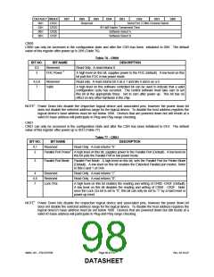
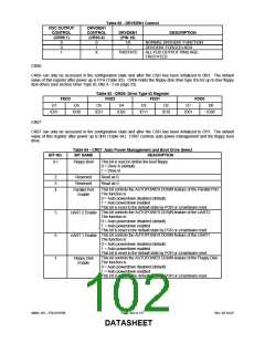
CR00
CR00 can only be accessed in the configuration state and after the CSR has been initialized to 00H. The default
value of this register after power up is 28H (Table 76).
Table 76 - CR00
BIT NO.
BIT NAME
Reserved
FDC Power 1
DESCRIPTION
0:2
3
Read Only. A read returns 0
A high level on this bit, supplies power to the FDC (default). A low level on this
bit puts the FDC in low power mode.
4,5,6
7
Reserved
Valid
Read only. A read returns bit 5 as a 1 and bits 4 and 6 as a 0.
A high level on this software controlled bit can be used to indicate that a valid
configuration cycle has occurred. The control software must take care to set
this bit at the appropriate times. Set to zero after power up. This bit has no
effect on any other hardware in the chip.
NOTE1: Power Down bits disable the respective logical device and associated pins, however the power down bit
does not disable the selected address range for the logical device. To disable the host address registers the
logical device’s base address must be set below 100h. Devices that are powered down but still reside at a
valid I/O base address will participate in Plug-and-Play range checking.
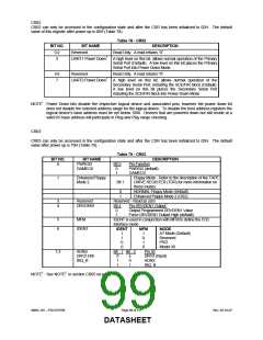
CR01
CR01 can only be accessed in the configuration state and after the CSR has been initialized to 01H. The default
value of this register after power up is 9CH (Table 77).
Table 77 - CR01
BIT NO.
BIT NAME
Reserved
DESCRIPTION
0,1
2
Read Only. A read returns “0”.
Parallel Port Power1 A high level on this bit, supplies power to the Parallel Port (Default). A low level on
this bit puts the Parallel Port in low power mode.
3
Parallel Port Mode
Parallel Port Mode. A high level on this bit, sets the Parallel Port for Printer Mode
(Default). A low level on this bit enables the Extended Parallel port modes. Refer
to Bits 0 and 1 of CR4
4
5,6
7
Reserved
Reserved
Lock CRx
Read Only. A read returns “1”.
Read Only. A read returns “0”.
A high level on this bit enables the reading and writing of CR00 -CR2F (Default).
A low level on this bit disables the reading and writing of CR00 - CR2F. Note:
once the Lock Crx bit is set to “0”, this bit can only be set to “1” by a hard reset or
power-up reset.
NOTE1 Power Down bits disable the respective logical device and associated pins, however the power down bit
does not disable the selected address range for the logical device. To disable the host address registers the
logical device’s base address must be set below 100h. Devices that are powered down but still reside at a
valid I/O base address will participate in Plug-and-Play range checking.
SMSC DS – FDC37N769
Page 98 of 137
Rev. 02-16-07
DATASHEET

 SMSC [ SMSC CORPORATION ]