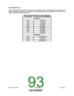
Wake Up From Auto Powerdown
If the FDC enters the powerdown state through the auto powerdown mode, wake up will occur after a reset or by
access to the specific registers shown below. If a hardware or software reset is used the part will follow the normal
reset sequence. If wake up occurs as a result of access through selected registers the FDC37N769 will resume
normal operation as if the FDC had never powered-down.
The following register accesses will wake up the FDC:
1. Enabling any one of the motor enable bits in the DOR register (reading the DOR does not awaken the
part).
2. A read from the MSR register.
3. A read or write to the Data register.
Once awake, the FDC37N769 will reinitiate the auto powerdown timer for 10ms. The FDC will powerdown again
when all of the powerdown conditions are met.
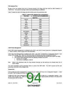
Register Behavior
Table 71 reiterates the available FDC PC/AT and PS/2, including Model 30 mode, registers. In order to maintain
software transparency, access to all the registers must be maintained regardless of the power state. As Table 71
shows, two kinds of registers are identified based on whether access results in the FDC remaining in the powerdown
state or not.
Registers that will not awaken the FDC can be accessed during powerdown without changing the powerdown state
but will reflect the true register status as shown in the FDC register description. For example, a write to one of these
registers will result in the FDC retaining the data and subsequently using it appropriately when the block reawakens.
During powerdown accessing FDC registers that do not affect the power state may increase device power
consumption, but only until the register access has been completed.
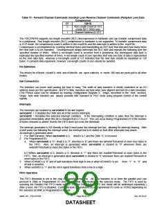
Table 71 - Available FDC PC/AT and PS/2 Registers
AVAILABLE REGISTERS
BASE + ADDRESS
PC-AT
PS/2 (Model 30)
ACCESS
PERMITTED
Access to these registers DOES NOT wake up the FDC
00H
01H
02H
03H
04H
06H
07H
07H
----
----
DOR1
SRA
SRB
DOR1
---
R
R
R/W
---
W
---
DSR1
---
DSR1
---
---
R
DIR
CCR
DIR
CCR
W
Access to these registers wakes up the FDC
04H
05H
MSR
MSR
R
DATA
DATA
R/W
Note1
Writing to any of the motor enable bits in the DOR or doing a software reset via the DOR or DSR reset bits
will wake up the FDC. Writing to any other DOR or DSR bits will not wake up the FDC.
Pin Behavior
The FDC37N769 is specifically designed for portable PC systems where power conservation is a primary concern.
Consequently, the behavior of the device pins during powerdown very important.
The pins of the FDC37N769 FDC can be divided into two major categories: system interface and floppy disk drive
interface. When the FDC is powered down, the floppy disk drive pins are disabled so that no power will be drawn
through the part as a result of any voltage applied to the pin within the part’s power supply range. Most of the system
interface pins are left active to monitor system accesses that are intended to wake up the floppy controller.
SMSC DS – FDC37N769
Page 92 of 137
Rev. 02-16-07
DATASHEET

 SMSC [ SMSC CORPORATION ]