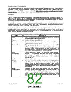
During an EPP cycle, if STROBE is active, it overrides the EPP write signal forcing the PDx bus to always be in a
write mode and the nWRITE signal to always be asserted.
Software Constraints
Before an EPP cycle is executed, the software must ensure that the control register bit PCD is a logic “0” (i.e. a 04H
or 05H should be written to the Control port). If the user leaves PCD as a logic “1”, and attempts to perform an EPP
write, the chip is unable to perform the write (because PCD is a logic “1”) and will appear to perform an EPP read on
the parallel bus, no error is indicated.
EPP 1.9 Write
The timing for a write operation (address or data) is shown in timing diagram EPP 1.9 Write Data or Address cycle.
IOCHRDY is driven active low at the start of each EPP write and is released when it has been determined that the
write cycle can complete. The write cycle can complete under the following circumstances:
1. If the EPP bus is not ready (nWAIT is active low) when nDATASTB or nADDRSTB goes active then the write
can complete when nWAIT goes inactive high.
2. If the EPP bus is ready (nWAIT is inactive high) then the chip must wait for it to go active low before changing
the state of nDATASTB, nWRITE or nADDRSTB. The write can complete once nWAIT is determined inactive.
Write Sequence of operation
1. The host selects an EPP register, places data on the SData bus and drives nIOW active.
2. The chip drives IOCHRDY inactive (low).
3. If WAIT is not asserted, the chip must wait until WAIT is asserted.
4. The chip places address or data on PData bus, clears PDIR, and asserts nWRITE.
5. Chip asserts nDATASTB or nADDRSTRB indicating that PData bus contains valid information, and the WRITE
signal is valid.
6. Peripheral deasserts nWAIT, indicating that any setup requirements have been satisfied and the chip may
begin the termination phase of the cycle.
7. A) The chip deasserts nDATASTB or nADDRSTRB, this marks the beginning of the termination
If it has not already done so, the peripheral should latch the information byte now.
phase.
B) The chip latches the data from the SData bus for the PData bus and asserts (releases) IOCHRDY allowing
the host to complete the write cycle.
8. Peripheral asserts nWAIT, indicating to the host that any hold time requirements have been satisfied and
acknowledging the termination of the cycle.
9. Chip may modify nWRITE and nPDATA in preparation for the next cycle.
EPP 1.9 Read
The timing for a read operation (data) is shown in timing diagram EPP Read Data cycle. IOCHRDY is driven active
low at the start of each EPP read and is released when it has been determined that the read cycle can complete. The
read cycle can complete under the following circumstances:
1. If the EPP bus is not ready (nWAIT is active low) when nDATASTB goes active then the read can complete
when nWAIT goes inactive high.
2. If the EPP bus is ready (nWAIT is inactive high) then the chip must wait for it to go active low before changing
the state of WRITE or before nDATASTB goes active. The read can complete once nWAIT is determined
inactive.
Read Sequence of Operation
1. The host selects an EPP register and drives nIOR active.
2. The chip drives IOCHRDY inactive (low).
3. If WAIT is not asserted, the chip must wait until WAIT is asserted.
4. The chip tri-states the PData bus and deasserts nWRITE.
5. Chip asserts nDATASTB or nADDRSTRB indicating that PData bus is tri-stated, PDIR is set and the nWRITE
signal is valid.
6. Peripheral drives PData bus valid.
7. Peripheral deasserts nWAIT, indicating that PData is valid and the chip may begin the termination phase of
the cycle.
8. A) The chip latches the data from the
nADDRSTRB, this marks the beginning of the termination phase.
B) The chip drives the valid data onto the SData bus and asserts (releases) IOCHRDY allowing the host to
complete the read cycle.
PData bus for the SData bus, deasserts
DATASTB or
9. Peripheral tri-states the PData bus and asserts nWAIT, indicating to the host that the PData bus is tri-stated.
10. Chip may modify nWRITE, PDIR and nPDATA in preparation for the next cycle.
SMSC DS – FDC37N769
Page 78 of 137
Rev. 02-16-07
DATASHEET

 SMSC [ SMSC CORPORATION ]