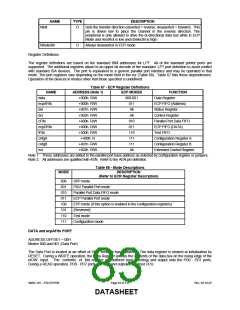
EPP 1.7 OPERATION
When the EPP 1.7 mode is selected in the configuration register, the standard and bi-directional modes are also
available. If no EPP Read, Write or Address cycle is currently executing, then the PDx bus is in the standard or bi-
directional mode, and all output signals (STROBE, AUTOFD, INIT) are as set by the SPP Control Port and direction is
controlled by PCD of the Control port.
In EPP mode, the system timing is closely coupled to the EPP timing. For this reason, a watchdog timer is required to
prevent system lockup. The timer indicates if more than 10usec have elapsed from the start of the EPP cycle (nIOR
or nIOW asserted) to the end of the cycle nIOR or nIOW deasserted). If a time-out occurs, the current EPP cycle
is aborted and the time-out condition is indicated in Status bit 0.
Software Constraints
Before an EPP cycle is executed, the software must ensure that the control register bits D0, D1 and D3 are set to
zero. Also, bit D5 (PCD) is a logic “0” for an EPP write or a logic “1” for and EPP read.
EPP 1.7 Write
The timing for a write operation (address or data) is shown in timing diagram EPP 1.7 Write Data or Address cycle.
IOCHRDY is driven active low when nWAIT is active low during the EPP cycle. This can be used to extend the
cycle time. The write cycle can complete when nWAIT is inactive high.
Write Sequence of Operation
1. The host sets PDIR bit in the control register to a logic “0”. This asserts nWRITE.
2. The host selects an EPP register, places data on the SData bus and drives nIOW active.
3. The chip places address or data on PData bus.
4. Chip asserts nDATASTB or nADDRSTRB indicating that PData bus contains valid information, and the WRITE
signal is valid.
5. If nWAIT is asserted, IOCHRDY is deasserted until the peripheral deasserts nWAIT or a time-out occurs.
6. When the host deasserts nI0W the chip deasserts nDATASTB or nADDRSTRB and latches the data from the
SData bus for the PData bus.
7. Chip may modify nWRITE, PDIR and nPDATA in preparation of the next cycle.
EPP 1.7 Read
The timing for a read operation (data) is shown in timing diagram EPP 1.7 Read Data cycle. IOCHRDY is driven
active low when nWAIT is active low during the EPP cycle. This can be used to extend the cycle time. The read
cycle can complete when nWAIT is inactive high.
Read Sequence of Operation
1. The host sets PDIR bit in the control register to a logic “1”. This deasserts nWRITE and tri-states the PData bus.
2. The host selects an EPP register and drives nIOR active.
3. Chip asserts nDATASTB or nADDRSTRB indicating that PData bus is tri-stated, PDIR is set and the nWRITE
signal is valid.
4. If nWAIT is asserted, IOCHRDY is deasserted until the peripheral deasserts nWAIT or a time-out occurs.
5. The Peripheral drives PData bus valid.
6. The Peripheral deasserts nWAIT, indicating that PData is valid and the chip may begin the termination phase of
the cycle.
7. When the host deasserts nI0R the chip deasserts nDATASTB or nADDRSTRB.
8. Peripheral tri-states the PData bus.
9. Chip may modify nWRITE, PDIR and nPDATA in preparation of the next cycle.
Table 64 - EPP Pin Descriptions
EPP
SIGNAL
EPP NAME
TYPE
DESCRIPTION
nWRITE
nWrite
O
This signal is active low. It denotes a write operation.
PD<0:7>
INTR
Address/Data
Interrupt
I/O
I
Bi-directional EPP byte wide address and data bus.
This signal is active high and positive edge triggered. (Pass
through with no inversion, Same as SPP).
SMSC DS – FDC37N769
Page 79 of 137
Rev. 02-16-07
DATASHEET

 SMSC [ SMSC CORPORATION ]