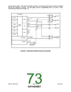
BIT 4 IRQE - INTERRUPT REQUEST ENABLE
The interrupt request enable bit when set to a high level may be used to enable interrupt requests from the Parallel
Port to the CPU. An interrupt request is generated on the IRQ port by a positive going nACK input. When the
IRQE bit is programmed low the IRQ is disabled.
BIT 5 PCD - PARALLEL CONTROL DIRECTION
Parallel Control Direction is valid in extended mode only (CR#1<3>=0). In printer mode, the direction is always out
regardless of the state of this bit. In bi-directional mode, a logic “0” means that the printer port is in output mode
(write); a logic “1” means that the printer port is in input mode (read).
Bits 6 and 7 during a read are a low level, and cannot be written.
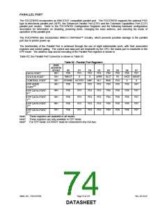
EPP ADDRESS PORT
ADDRESS OFFSET = 03H
The EPP Address Port is located at an offset of ‘03H’ from the base address. The address register is cleared at
initialization by RESET. During a WRITE operation, the contents of DB0-DB7 are buffered (non inverting) and output
onto the PD0 - PD7 ports, the leading edge of nIOW causes an EPP ADDRESS WRITE cycle to be performed,
the trailing edge of IOW latches the data for the duration of the EPP write cycle. During a READ operation, PD0 -
PD7 ports are read, the leading edge of IOR causes an EPP ADDRESS READ cycle to be performed and the data
output to the host CPU, the deassertion of ADDRSTB latches the PData for the duration of the IOR cycle. This
register is only available in EPP mode.
EPP DATA PORT 0
ADDRESS OFFSET = 04H
The EPP Data Port 0 is located at an offset of ‘04H’ from the base address. The data register is cleared at
initialization by RESET. During a WRITE operation, the contents of DB0-DB7 are buffered (non inverting) and output
onto the PD0 - PD7 ports, the leading edge of nIOW causes an EPP DATA WRITE cycle to be performed, the trailing
edge of IOW latches the data for the duration of the EPP write cycle. During a READ operation, PD0 - PD7 ports are
read, the leading edge of IOR causes an EPP READ cycle to be performed and the data output to the host CPU, the
deassertion of DATASTB latches the PData for the duration of the IOR cycle. This register is only available in EPP
mode.
EPP DATA PORT 1
ADDRESS OFFSET = 05H
The EPP Data Port 1 is located at an offset of ‘05H’ from the base address. Refer to EPP DATA PORT 0 for a
description of operation. This register is only available in EPP mode.
EPP DATA PORT 2
ADDRESS OFFSET = 06H
The EPP Data Port 2 is located at an offset of ‘06H’ from the base address. Refer to EPP DATA PORT 0 for a
description of operation. This register is only available in EPP mode.
EPP DATA PORT 3
ADDRESS OFFSET = 07H
The EPP Data Port 3 is located at an offset of ‘07H’ from the base address. Refer to EPP DATA PORT 0 for a
description of operation. This register is only available in EPP mode.
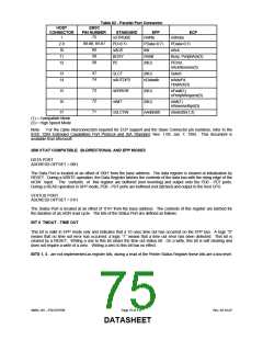
EPP 1.9 OPERATION
When the EPP mode is selected in the configuration register, the standard and bi-directional modes are also
available. If no EPP Read, Write or Address cycle is currently executing, then the PDx bus is in the standard or bi-
directional mode, and all output signals (STROBE, AUTOFD, INIT) are as set by the SPP Control Port and direction is
controlled by PCD of the Control port.
In EPP mode, the system timing is closely coupled to the EPP timing. For this reason, a watchdog timer is required to
prevent system lockup. The timer indicates if more than 10μsec have elapsed from the start of the EPP cycle (nIOR
or nIOW asserted) to nWAIT being deasserted (after command). If a time-out occurs, the current EPP cycle is
aborted and the time-out condition is indicated in Status bit 0.
SMSC DS – FDC37N769
Page 77 of 137
Rev. 02-16-07
DATASHEET

 SMSC [ SMSC CORPORATION ]