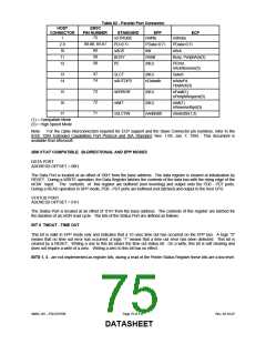
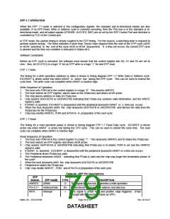
Table 63 - Parallel Port Connector
HOST
SMSC
CONNECTOR
PIN NUMBER
STANDARD
nSTROBE
EPP
nWrite
ECP
75
1
nStrobe
69-66, 64-61
2-9
10
11
12
PD<0:7>
nACK
BUSY
PE
PData<0:7>
Intr
PData<0:7>
nAck
60
59
58
nWait
Busy, PeriphAck(3)
(NU)
PError,
nAckReverse(3)
57
74
13
14
SLCT
(NU)
Select
nAUTOFD
nDatastb
nAutoFd,
HostAck(3)
73
72
71
15
16
17
nERROR
nINIT
(NU)
nFault(1)
nPeriphRequest(3)
(NU)
nInit(1)
nReverseRqst(3)
nSLCTIN
nAddrstrb
nSelectIn(1,3)
(1) = Compatible Mode
(3) = High Speed Mode
Note:
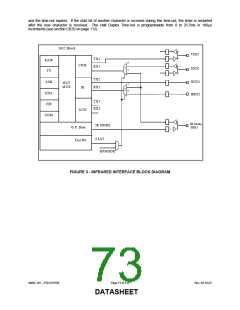
For the cable interconnection required for ECP support and the Slave Connector pin numbers, refer to the
IEEE 1284 Extended Capabilities Port Protocol and ISA Standard, Rev. 1.09, Jan. 7, 1993. This document is
available from Microsoft.
IBM XT/AT COMPATIBLE, BI-DIRECTIONAL AND EPP MODES
DATA PORT
ADDRESS OFFSET = 00H
The Data Port is located at an offset of ‘00H’ from the base address. The data register is cleared at initialization by
RESET. During a WRITE operation, the Data Register latches the contents of the data bus with the rising edge of the
nIOW input. The contents of this register are buffered (non inverting) and output onto the PD0 - PD7 ports.
During a READ operation in SPP mode, PD0 - PD7 ports are buffered (not latched) and output to the host CPU.
STATUS PORT
ADDRESS OFFSET = 01H
The Status Port is located at an offset of ‘01H’ from the base address. The contents of this register are latched for
the duration of an nIOR read cycle. The bits of the Status Port are defined as follows:
BIT 0 TMOUT - TIME OUT
This bit is valid in EPP mode only and indicates that a 10 usec time out has occurred on the EPP bus. A logic “0”
means that no time out error has occurred; a logic “1” means that a time out error has been detected. This bit is
cleared by a RESET. Writing a one to this bit clears the time out status bit. On a write, this bit is self clearing and
does not require a write of a zero. Writing a zero to this bit has no effect.
BITS 1, 2 - are not implemented as register bits, during a read of the Printer Status Register these bits are a low level.
SMSC DS – FDC37N769
Page 75 of 137
Rev. 02-16-07
DATASHEET

 SMSC [ SMSC CORPORATION ]