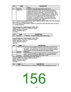
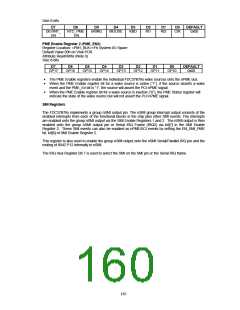
Size:8-bits
D7
DEVINT_
EN
D6
RTC_PME
_EN
D5
nRING
D4
MOUSE
D3
KBD
D2
RI1
D1
RI2
D0
CIR
DEFAULT
0x00
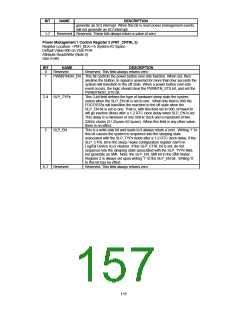
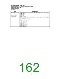
PME Enable Register 2 (PME_EN2)
Register Location: <PM1_BLK>+Fh System I/O Space
Default Value:00h on Vbat POR
Attribute:Read/Write (Note 0)
Size:8-bits
D7
GP17
D6
GP16
D5
GP15
D4
GP14
D3
GP13
D2
GP12
D1
GP11
D0
GP10
DEFAULT
0x00
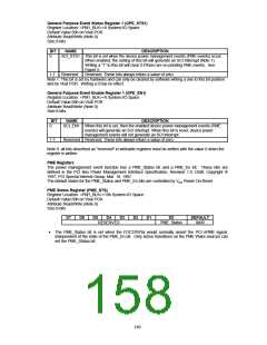
•
•
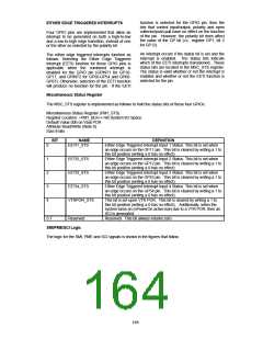
The PME Enable registers enable the individual FDC37B78x wake sources onto the nPME bus.
When the PME Enable register bit for a wake source is active (“1”), if the source asserts a wake
event and the PME_En bit is “1”, the source will assert the PCI nPME signal.
•
When the PME Enable register bit for a wake source is inactive (“0”), the PME Status register will
indicate the state of the wake source but will not assert the PCI nPME signal.
SMI Registers
The FDC37B78x implements a group nSMI output pin. The nSMI group interrupt output consists of the
enabled interrupts from each of the functional blocks in the chip plus other SMI events. The interrupts
are enabled onto the group nSMI output via the SMI Enable Registers 1 and 2. The nSMI output is then
enabled onto the group nSMI output pin or Serial IRQ Frame (IRQ2) via bit[7] in the SMI Enable
Register 2. These SMI events can also be enabled as nPME/SCI events by setting the EN_SMI_PME
bit, bit[6] of SMI Enable Register 2.
This register is also used to enable the group nSMI output onto the nSMI Serial/Parallel IRQ pin and the
routing of 8042 P12 internally to nSMI.
The IRQ mux Register Bit 7 is used to select the SMI on the SMI pin or the Serial IRQ frame.
162

 SMSC [ SMSC CORPORATION ]