Fan Control Device with High Frequency PWM Support and Hardware Monitoring Features
Datasheet
This register contains the following bits:
Bit[0] Low-Power Mode Select
0= Sleep Mode (default)
1= Shutdown Mode
Bit[1] Monitoring Mode Select
0= Continuous Monitor Mode (default)
1= Cycle Monitor Mode
Bit[2] INT# Enable
0=Disables INT# pin output function (default)
1=Enables INT# pin output function
Bit[3] SMSC Reserved
This is a read/write bit. Reading this bit has no effect. Writing this bit to ‘1’ may cause unwanted
results.
Bit [4] SMSC Reserved
This is a read/write bit. Reading this bit has no effect. Writing this bit to ‘1’ may cause
unwanted results.
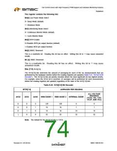
Bits [7:5] AVG[2:0]
The AVG[2:0] bits determine the amount of averaging for each of the six measurements that are
performed by the hardware monitor before the reading registers are updated (Table 8.43, "AVG[2:0] Bit
Decoder"). The AVG[2:0] bits are priority encoded where the most significant bit has highest priority.
For example, when the AVG2 bit is asserted, 32 averages will be performed for each measurement
before the reading registers are updated regardless of the state of the AVG[1:0] bits.
Table 8.43 AVG[2:0] Bit Decoder
SFTR[7:5]
AVERAGES PER READING
ALL VOLTAGE
READINGS
AVG2
AVG1
AVG0
REM DIODE 1 REM DIODE 2
INTERNAL DIODE
(+2.5V, +5V, +12V,
VCCP, AND VCC)
0
0
0
1
0
0
1
X
0
1
128
16
128
16
8
1
8
1
X
X
16
16
16
32
16
32
32
32
Note: The default for the AVG[2:0] bits is ‘010’b.
Revision 0.4 (04-04-05)
SMSC EMC6D103
DATA7S4HEET

 SMSC [ SMSC CORPORATION ]