Fan Control Device with High Frequency PWM Support and Hardware Monitoring Features
Datasheet
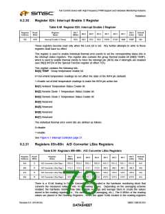
8.2.30
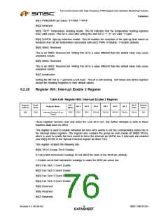
Register 82h: Interrupt Enable 3 Register
Table 8.49 Register 82h: Interrupt Enable 3 Register
Register
Address
Read/
Write
Register
Name
Bit 7
Bit 0
Default
Value
Bit 6
Bit 5
Bit 4
Bit 3
Bit 2
Bit 1
(MSb)
(LSb)
82h
R/W
Interrupt Enable 3 (Temp)
RES
RES
RES
RES
D2EN
D1EN
AMB
TEMP
0Eh
These registers become read only when the Lock bit is set. Any further attempts to write to these
registers shall have no effect.
This register is used to enable individual thermal error events to set the corresponding status bits in
the interrupt status registers. This register also contains the group thermal enable bit (Bit[0] TEMP),
which is used to enable thermal events to force the interrupt pin (INT#) low if interrupts are enabled
(see Bit[2] INTEN of the Special Function register at offset 7Ch).
This register contains the following bits:
Bit[0] TEMP. Group temperature enable bit.
0=Out-of-limit temperature readings do not affect the state of the INT# pin (default)
1=Enable out-of-limit temperature readings to make the INT# pin active low
Bit[1] Ambient Temperature Status Enable bit.
Bit[2] Remote Diode 1 Temperature Status Enable bit.
Bit[3] Remote Diode 2 Temperature Status Enable bit
Bit[4] Reserved
Bit[5] Reserved
Bit[6] Reserved
Bit[7] Reserved
The individual thermal error event bits are defined as follows:
0=disable
1=enable.
See Figure 6.1 Interrupt Controlon page 27.
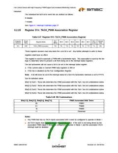
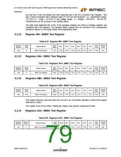
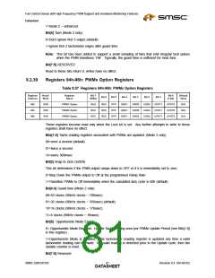
8.2.31
Registers 85h-88h: A/D Converter LSbs Registers
Table 8.50 Registers 85h-88h: A/D Converter LSbs Registers
Register
Address
Read/
Write
Register
Name
Bit 7
Bit 0
Default
Value
Bit 6
Bit 5
Bit 4
Bit 3
Bit 2
Bit 1
(MSb)
(LSb)
85h
86h
87h
88h
R
R
R
R
A/D Converter LSbs Reg 1
A/D Converter LSbs Reg 2
A/D Converter LSbs Reg 3
A/D Converter LSbs Reg 4
RD2.3
V12.3
V50.3
VCC.3
RD2.2
V12.2
V50.2
VCC.2
RD2.1
V12.1
V50.1
VCC.1
RD2.0
V12.0
V50.0
VCC.0
RD1.3
AM.3
RD1.2
AM.2
RD1.1
AM.1
RD1.0
AM.0
N/A
N/A
N/A
N/A
V25.3
VCP.3
V25.2
VCP.2
V25.1
VCP.1
V25.0
VCP.0
There is a 10-bit Analog to Digital Converter (ADC) located in the hardware monitoring block that
converts the measured voltages into 10-bit reading values. Depending on the averaging scheme
enabled, the hardware monitor may take multiple readings and average them to create the values
stored in the reading registers (i.e., 16x averaging, 32x averaging, etc.) The 8 MSb’s of the reading
values are placed in the Reading Registers. When the upper 8-bits located in the reading registers
Revision 0.4 (04-04-05)
SMSC EMC6D103
DATA7S8HEET

 SMSC [ SMSC CORPORATION ]