Legacy-Free Keyboard/Embedded Controller with SPI and LPC Docking Interface
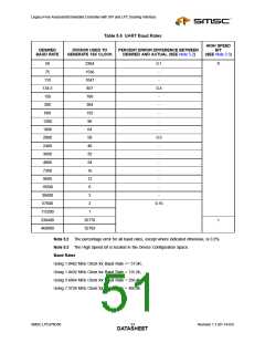
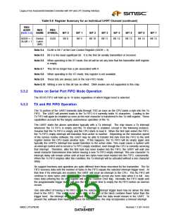
Table 5.8 Register Summary for an Individual UART Channel (continued)
REG
ADDR
REG
REG
(Note 5.4)
NAME
SYMBOL
BIT 0
BIT 1
BIT 2
BIT 3
BIT 4
BIT 5
BIT 6
BIT 7
ADDR = 1 Divisor
DLM
Bit 8
Bit 9
Bit 10
Bit 11
Bit 12
Bit 13
Bit 14
Bit 15
DLAB = 1
Latch
(MS)
Note 5.4 DLAB is Bit 7 of the Line Control Register (ADDR = 3).
Note 5.5 Bit 0 is the least significant bit. It is the first bit serially transmitted or received.
Note 5.6 When operating in the XT mode, this bit will be set any time that the transmitter shift register
is empty.
Note 5.7 This bit no longer has a pin associated with it.
Note 5.8 When operating in the XT mode, this register is not available.
Note 5.9 These bits are always zero in the non-FIFO mode.
Note 5.10 Writing a one to this bit has no effect. DMA modes are not supported in this chip.
5.3.2
5.3.3
Notes on Serial Port FIFO Mode Operation
The RCVR FIFO will hold up to 16 bytes regardless of which trigger level is selected.
TX and RX FIFO Operation
The Tx portion of the UART transmits data through TXD as soon as the CPU loads a byte into the Tx
FIFO. The UART will prevent loads to the Tx FIFO if it currently holds 16 characters. Loading to the
Tx FIFO will again be enabled as soon as the next character is transferred to the Tx shift register. These
capabilities account for the largely autonomous operation of the Tx.
The UART starts the above operations typically with a Tx interrupt. The chip issues a Tx interrupt
whenever the Tx FIFO is empty and the Tx interrupt is enabled, except in the following instance.
Assume that the Tx FIFO is empty and the CPU starts to load it. When the first byte enters the FIFO,
the Tx FIFO empty interrupt will transition from active to inactive. Depending on the execution speed
of the service routine software, the UART may be able to transfer this byte from the FIFO to the shift
register before the CPU loads another byte. If this happens, the Tx FIFO will be empty again and
typically the UART's interrupt line would transition to the active state. This could cause a system with
an interrupt control unit to record a Tx FIFO empty condition, even though the CPU is currently servicing
that interrupt. Therefore, after the first byte has been loaded into the FIFO, the UART will wait one
serial character transmission time before issuing a new Tx FIFO empty interrupt. This one character Tx
interrupt delay will remain active until at least two bytes have been loaded into the FIFO, concurrently.
When the Tx FIFO empties after this condition, the Tx interrupt will be activated without a one character
delay.
Rx support functions and operation are quite different from those described for the transmitter. The Rx
FIFO receives data until the number of bytes in the FIFO equals the selected interrupt trigger level. At
that time if Rx interrupts are enabled, the UART will issue an interrupt to the CPU. The Rx FIFO will
continue to store bytes until it holds 16 of them. It will not accept any more data when it is full. Any
more data entering the Rx shift register will set the Overrun Error flag. Normally, the FIFO depth and
the programmable trigger levels will give the CPU ample time to empty the Rx FIFO before an overrun
occurs.
One side-effect of having a Rx FIFO is that the selected interrupt trigger level may be above the data
level in the FIFO. This could occur when data at the end of the block contains fewer bytes than the
trigger level. No interrupt would be issued to the CPU and the data would remain in the UART. To
prevent the software from having to check for this situation, the chip incorporates a timeout interrupt.
SMSC LPC47N350
Revision 1.1 (01-14-03)
DATA3S7HEET

 SMSC [ SMSC CORPORATION ]